Register 12: GPIO 4-mA Drive Select (GPIODR4R), offset 0x504
The GPIODR4R register is the 4-mA drive control register. Each GPIO signal in the port can be
individually configured without affecting the other pads. When setting the DRV4 bit for a GPIO signal,
the corresponding DRV2 bit in the GPIODR2R register and DRV8 bit in the GPIODR8R register are
automatically cleared by hardware.
Note: This register has no effect on port pins PL6 and PL7.
GPIO 4-mA Drive Select (GPIODR4R)
GPIO Port A (AHB) base: 0x4005.8000
GPIO Port B (AHB) base: 0x4005.9000
GPIO Port C (AHB) base: 0x4005.A000
GPIO Port D (AHB) base: 0x4005.B000
GPIO Port E (AHB) base: 0x4005.C000
GPIO Port F (AHB) base: 0x4005.D000
GPIO Port G (AHB) base: 0x4005.E000
GPIO Port H (AHB) base: 0x4005.F000
GPIO Port J (AHB) base: 0x4006.0000
GPIO Port K (AHB) base: 0x4006.1000
GPIO Port L (AHB) base: 0x4006.2000
GPIO Port M (AHB) base: 0x4006.3000
GPIO Port N (AHB) base: 0x4006.4000
GPIO Port P (AHB) base: 0x4006.5000
GPIO Port Q (AHB) base: 0x4006.6000
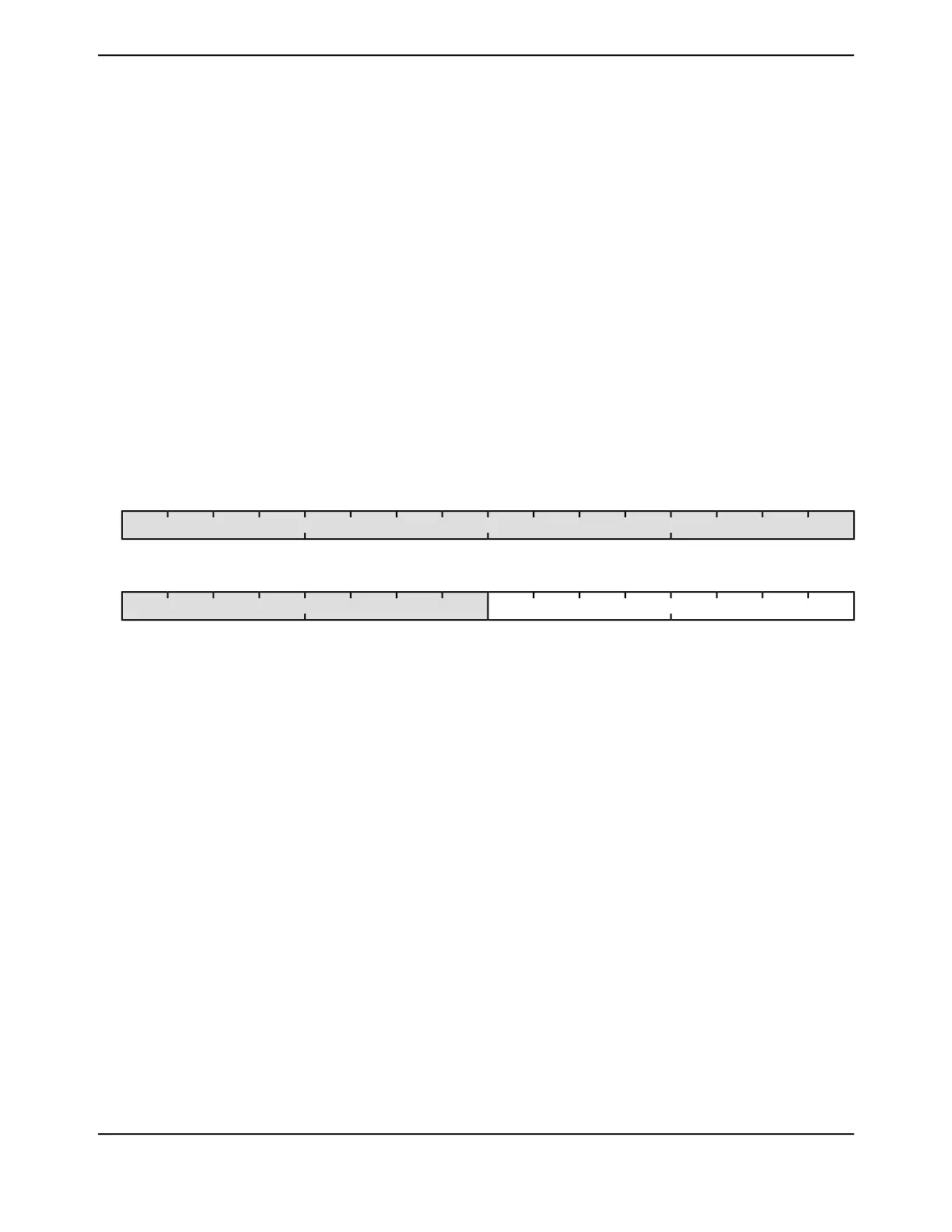
Offset 0x504
Type RW, reset 0x0000.0000
16171819202122232425262728293031
reserved
ROROROROROROROROROROROROROROROROType
0000000000000000Reset
0123456789101112131415
DRV4reserved
RWRWRWRWRWRWRWRWROROROROROROROROType
0000000000000000Reset
DescriptionResetTypeNameBit/Field
Software should not rely on the value of a reserved bit. To provide
compatibility with future products, the value of a reserved bit should be
preserved across a read-modify-write operation.
0x0000.00ROreserved31:8
Output Pad 4-mA Drive Enable
DescriptionValue
The drive for the corresponding GPIO pin is controlled by the
GPIODR2R or GPIODR8R register.
0
The corresponding GPIO pin has 4-mA drive.1
Setting a bit in either the GPIODR2 register or the GPIODR8 register
clears the corresponding 4-mA enable bit. The change is effective on
the next clock cycle.
0x00RWDRV47:0
773June 18, 2014
Texas Instruments-Production Data
Tiva
™
TM4C1294NCPDT Microcontroller
 Loading...


