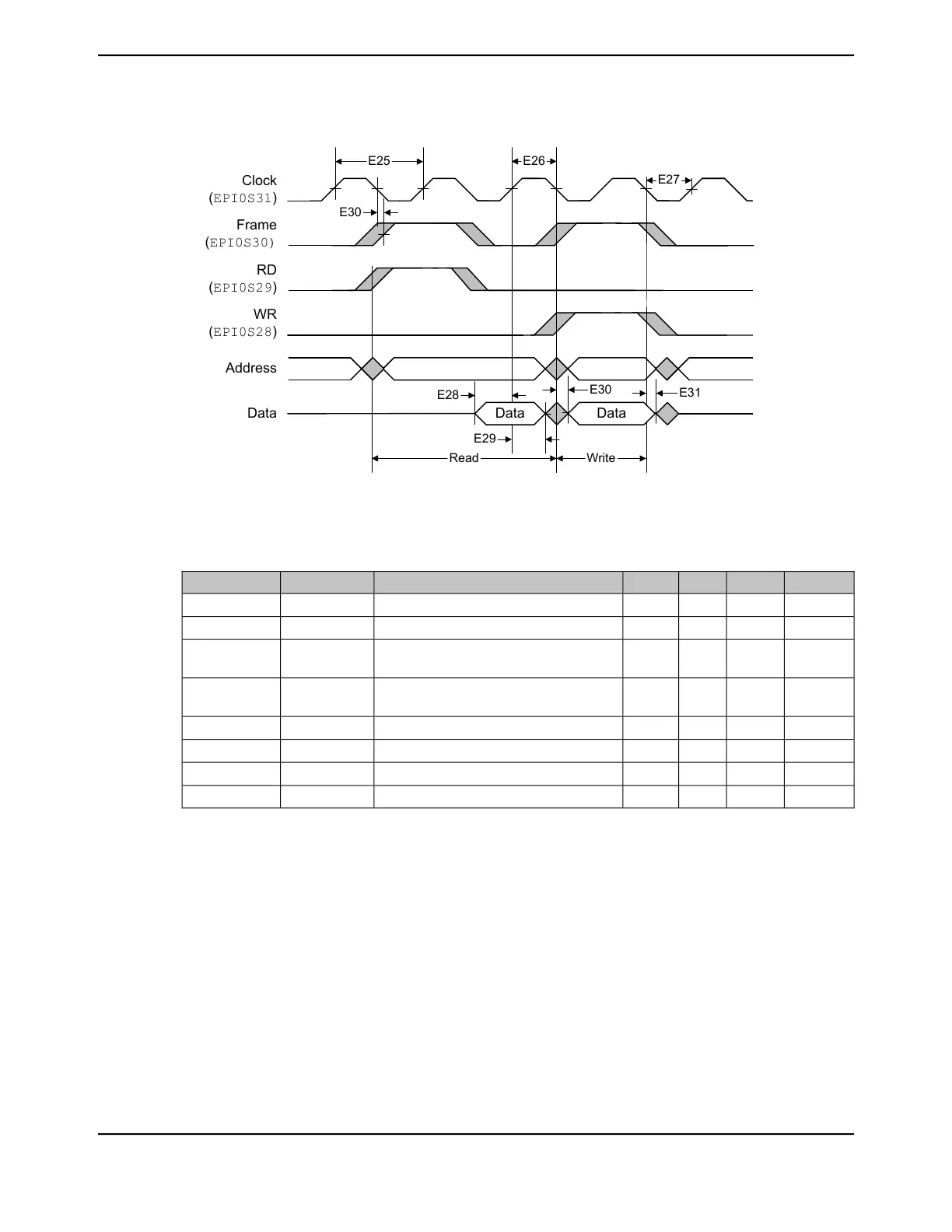
Figure 27-25. General-Purpose Mode Read and Write Timing
Read
E28
E31
E25
E27
E30
Clock
(EPI0S31)
Frame
(EPI0S30)
RD
(EPI0S29)
WR
(EPI0S28)
Address
Data
E29
E30
Write
Data Data
E26
Note: This figure illustrates accesses where the FRM50 bit is clear, the FRMCNT field is 0x0 and the
WR2CYC bit is clear.
Table 27-43. EPI PSRAM Interface Characteristics
UnitMaxNomMinParameter NameParameterParameter No
ns--20EPI_CLK periodT
EPICLK
E33
ns1.8--EPI_CLK rise or fall timeT
RTFT
E34
ns20-4.5Falling EPI_CLK to Address/Write Data or
Control output valid
a
T
OV
E35
ns--2Falling EPI_CLK to Address/Write Data or
Control hold time
a
T
HT
E36
ns9--Read data setup time from EPI_CLK risingT
SUP
E37
ns--0Read data output hold from EPI_CLK risingT
DH
E38
ns9--iRDY setup timeT
IRV
E39
ns9--iRDY hold timeT
IRH
E40
a. Control output includes WRn, RDn, OEn, BSELn, ALE, and CSn.
June 18, 20141858
Texas Instruments-Production Data
Electrical Characteristics
 Loading...


