15.4.2 Sample Sequencer Configuration
Configuration of the sample sequencers is slightly more complex than the module initialization
because each sample sequencer is completely programmable.
The configuration for each sample sequencer should be as follows:
1. Ensure that the sample sequencer is disabled by clearing the corresponding ASENn bit in the
ADCACTSS register. Programming of the sample sequencers is allowed without having them
enabled. Disabling the sequencer during programming prevents erroneous execution if a trigger
event were to occur during the configuration process.
2. Configure the trigger event for the sample sequencer in the ADCEMUX register.
3. When using a PWM generator as the trigger source, use the ADC Trigger Source Select
(ADCTSSEL) register to specify in which PWM module the generator is located. The default
register reset selects PWM module 0 for all generators.
4. For each sample in the sample sequence, configure the corresponding input source in the
ADCSSMUXn and ADCSSEMUXn registers.
5. For each sample in the sample sequence, configure the sample control bits in the corresponding
nibble in the ADCSSCTLn register. When programming the last nibble, ensure that the END bit
is set. Failure to set the END bit causes unpredictable behavior.
6. If interrupts are to be used, set the corresponding MASK bit in the ADCIM register.
7. Enable the sample sequencer logic by setting the corresponding ASENn bit in the ADCACTSS
register.
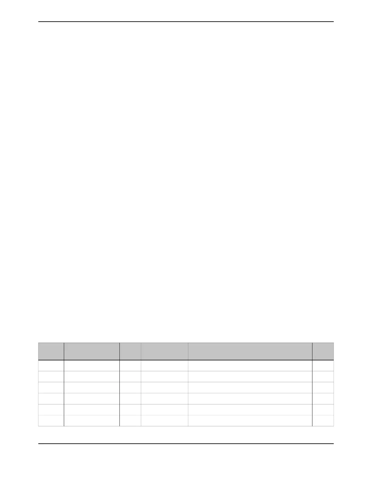
15.5 Register Map
Table 15-7 on page 1073 lists the ADC registers. The offset listed is a hexadecimal increment to the
register's address, relative to that ADC module's base address of:
■ ADC0: 0x4003.8000
■ ADC1: 0x4003.9000
Note that the ADC module clock must be enabled before the registers can be programmed (see
page 396). There must be a delay of 3 system clocks after the ADC module clock is enabled before
any ADC module registers are accessed.
Table 15-7. ADC Register Map
See
page
DescriptionResetTypeNameOffset
1077ADC Active Sample Sequencer0x0000.0000RWADCACTSS0x000
1079ADC Raw Interrupt Status0x0000.0000ROADCRIS0x004
1082ADC Interrupt Mask0x0000.0000RWADCIM0x008
1085ADC Interrupt Status and Clear0x0000.0000RW1CADCISC0x00C
1089ADC Overflow Status0x0000.0000RW1CADCOSTAT0x010
1091ADC Event Multiplexer Select0x0000.0000RWADCEMUX0x014
1073June 18, 2014
Texas Instruments-Production Data
Tiva
™
TM4C1294NCPDT Microcontroller
 Loading...


