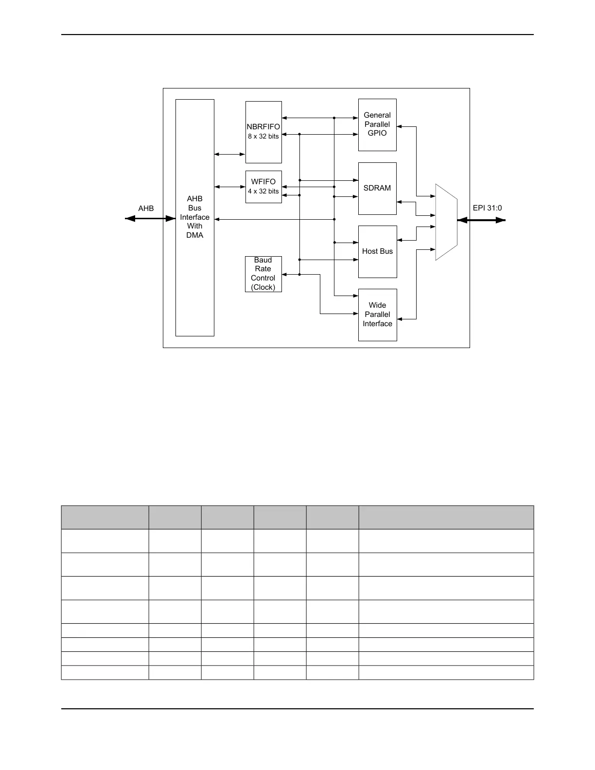
Figure 11-1. EPI Block Diagram
Baud
Rate
Control
(Clock)
AHB
Bus
Interface
With
DMA
Wide
Parallel
Interface
Host Bus
SDRAM
General
Parallel
GPIO
AHB
EPI 31:0
NBRFIFO
8 x 32 bits
WFIFO
4 x 32 bits
11.2 Signal Description
The following table lists the external signals of the EPI controller and describes the function of each.
The EPI controller signals are alternate functions for GPIO signals and default to be GPIO signals
at reset. The column in the table below titled "Pin Mux/Pin Assignment" lists the GPIO pin placement
for the EPI signals. The AFSEL bit in the GPIO Alternate Function Select (GPIOAFSEL) register
(page 770) should be set to choose the EPI controller function. The number in parentheses is the
encoding that must be programmed into the PMCn field in the GPIO Port Control (GPIOPCTL)
register (page 787) to assign the EPI signals to the specified GPIO port pins. For more information
on configuring GPIOs, see “General-Purpose Input/Outputs (GPIOs)” on page 742.
Table 11-1. External Peripheral Interface Signals (128TQFP)
DescriptionBuffer TypePin TypePin Mux / Pin
Assignment
Pin NumberPin Name
EPI module 0 signal 0.TTLI/OPK0 (15)
PH0 (15)
18
29
EPI0S0
EPI module 0 signal 1.TTLI/OPK1 (15)
PH1 (15)
19
30
EPI0S1
EPI module 0 signal 2.TTLI/OPK2 (15)
PH2 (15)
20
31
EPI0S2
EPI module 0 signal 3.TTLI/OPK3 (15)
PH3 (15)
21
32
EPI0S3
EPI module 0 signal 4.TTLI/OPC7 (15)22EPI0S4
EPI module 0 signal 5.TTLI/OPC6 (15)23EPI0S5
EPI module 0 signal 6.TTLI/OPC5 (15)24EPI0S6
EPI module 0 signal 7.TTLI/OPC4 (15)25EPI0S7
817June 18, 2014
Texas Instruments-Production Data
Tiva
™
TM4C1294NCPDT Microcontroller
 Loading...


