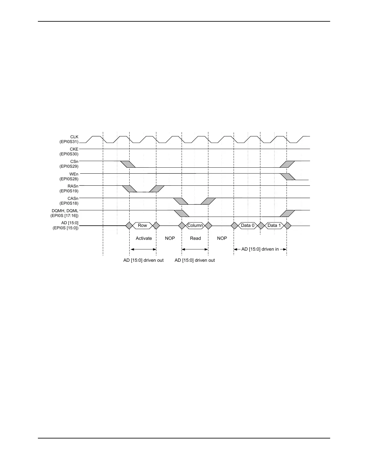
11.4.2.5 Normal Read Cycle
Figure 11-3 on page 825 shows a normal read cycle of n halfwords; n can be 1 or 2. The cycle begins
with the Activate command and the row address on the EPI0S[15:0] signals. With the programmed
CAS latency of 2, the Read command with the column address on the EPI0S[15:0] signals follows
after 2 clock cycles. Following one more NOP cycle, data is read in on the EPI0S[15:0] signals
on every rising clock edge. The DQMH, DQML, and CSn signals are deasserted after the last
halfword of data is received, signaling the end of the cycle. At least one clock period of inactivity
separates any two SDRAM cycles.
Figure 11-3. SDRAM Normal Read Cycle
Row Column Data 0 Data 1
CLK
(EPI0S31)
CKE
(EPI0S30)
CSn
(EPI0S29)
WEn
(EPI0S28)
RASn
(EPI0S19)
CASn
(EPI0S18)
DQMH, DQML
(EPI0S [17:16])
AD [15:0]
(EPI0S [15:0])
Activate NOP Read
NOP
AD [15:0] driven in
AD [15:0] driven out AD [15:0] driven out
11.4.2.6 Write Cycle
Figure 11-4 on page 826 shows a write cycle of n halfwords; n can be any number greater than or
equal to 1. The cycle begins with the Activate command and the row address on the EPI0S[15:0]
signals. With the programmed CAS latency of 2, the Write command with the column address on
the EPI0S[15:0] signals follows after 2 clock cycles. When writing to SDRAMs, the Write command
is presented with the first halfword of data. Because the address lines and the data lines are
multiplexed, the column address is modified to be (programmed address -1). During the Write
command, the DQMH and DQML signals are high, so no data is written to the SDRAM. On the next
clock, the DQMH and DQML signals are asserted, and the data associated with the programmed
address is written. The Burst Terminate command occurs during the clock cycle following the write
of the last halfword of data. The WEn, DQMH, DQML, and CSn signals are deasserted after the
last halfword of data is received, signaling the end of the access. At least one clock period of inactivity
separates any two SDRAM cycles.
825June 18, 2014
Texas Instruments-Production Data
Tiva
™
TM4C1294NCPDT Microcontroller
 Loading...


