27.16 Analog-to-Digital Converter (ADC)
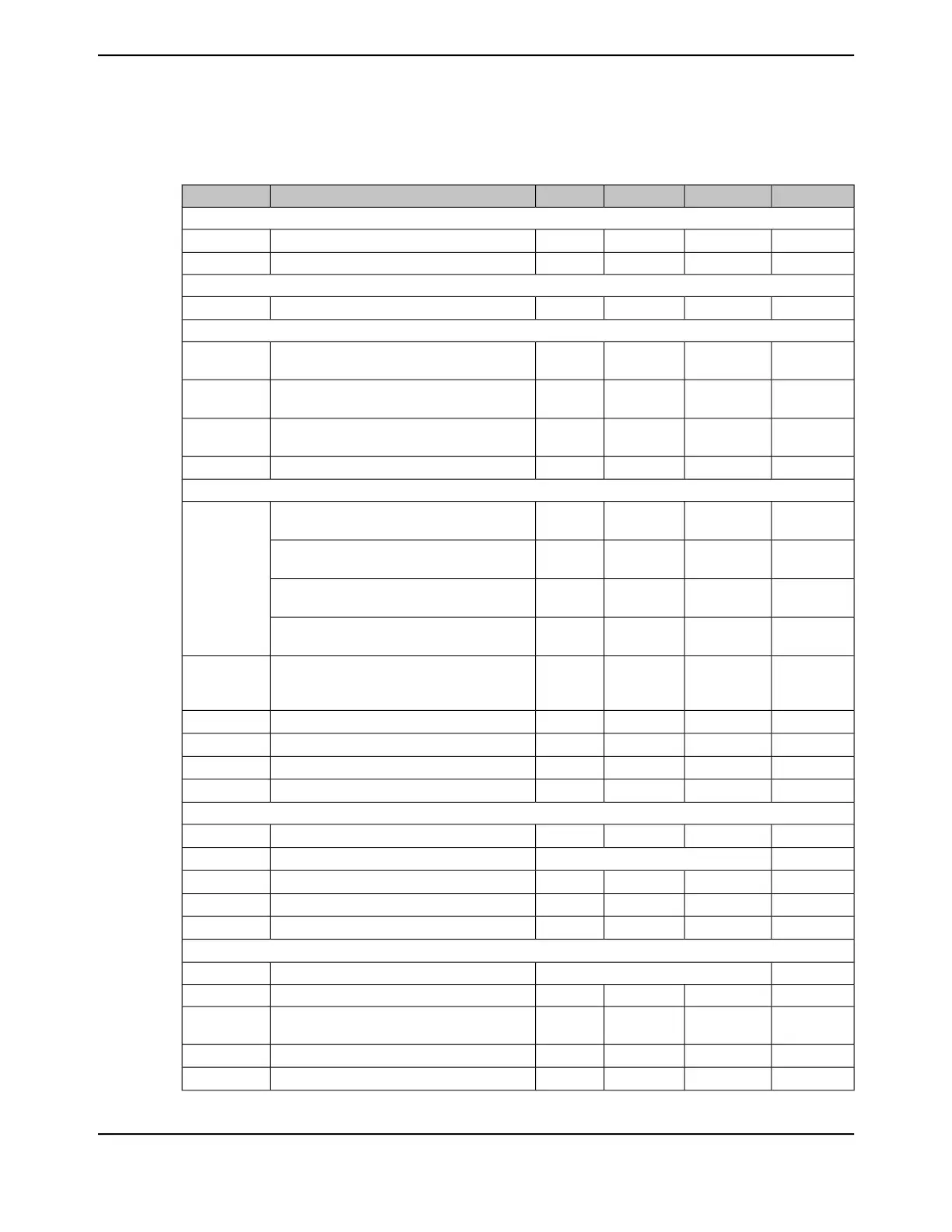
Table 27-44. ADC Electrical Characteristics for ADC at 1 Msps
ab
UnitMaxNomMinParameter NameParameter
POWER SUPPLY REQUIREMENTS
V3.633.32.97ADC supply voltageV
DDA
V-0-ADC ground voltageGNDA
VDDA / GNDA VOLTAGE REFERENCE
μF-1.0 // 0.01
c
-Voltage reference decoupling capacitanceC
REF
EXTERNAL VOLTAGE REFERENCE INPUT
VV
DDA
V
DDA
2.4Positive external voltage reference for ADC,
when VREF field in the ADCCTL register is 0x1-
V
REFA+
µA440330.5-Current on VREF+ input, using external V
REF+
=
3.3 V
I
VREF
µA2.0--DC leakage current on VREF+ input when
external VREF disabled
I
LVREF
μF-1.0 // 0.01
c
-External reference decoupling capacitanceC
REF
ANALOG INPUT
VV
DDA
-0Single-ended, full- scale analog input voltage,
internal reference
de
V
ADCIN
VV
VDDA
--V
DDA
Differential, full-scale analog input voltage,
internal reference
df
VV
REFA+
-GNDASingle-ended, full-scale analog input voltage,
external reference
e
VV
REFA+
-
GNDA
-- (V
REFA+
-
GNDA)
Differential, full-scale analog input voltage,
external reference
g
V[(V
REFA+
+
V
REFA-
) / 2] ±
0.025
--Input common mode voltage, differential mode
h
VIN
CM
µA2.0--ADC input leakage current
i
I
L
kΩ2.5--ADC equivalent input resistance
i
R
ADC
pF10--ADC equivalent input capacitance
i
C
ADC
Ω500--Analog source resistance
i
R
S
SAMPLING DYNAMICS
MHz-16-ADC conversion clock frequency
j
F
ADC
Msps1ADC conversion rateF
CONV
ns-250-ADC sample timeT
S
µs-1-ADC conversion time
k
T
C
ADC clocks-2-Latency from trigger to start of conversionT
LT
SYSTEM PERFORMANCE when using external reference
lm
bits12ResolutionN
LSB±3.0±1.5-Integral nonlinearity error, over full input rangeINL
LSB+2.0/-1.0
n
±0.8-Differential nonlinearity error, over full input
range
DNL
LSB±3.0±1.0-Offset errorE
O
LSB±3.0±2.0-Gain error
o
E
G
1861June 18, 2014
Texas Instruments-Production Data
Tiva
™
TM4C1294NCPDT Microcontroller
 Loading...


