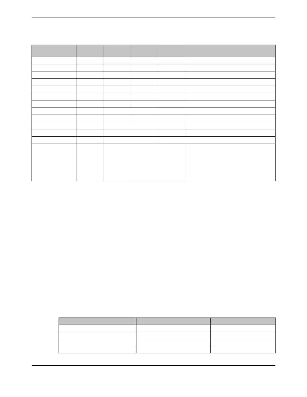
Table 15-1. ADC Signals (128TQFP) (continued)
DescriptionBuffer TypePin TypePin Mux / Pin
Assignment
Pin NumberPin Name
Analog-to-digital converter input 8.AnalogIPE5124AIN8
Analog-to-digital converter input 9.AnalogIPE4123AIN9
Analog-to-digital converter input 10.AnalogIPB4121AIN10
Analog-to-digital converter input 11.AnalogIPB5120AIN11
Analog-to-digital converter input 12.AnalogIPD34AIN12
Analog-to-digital converter input 13.AnalogIPD23AIN13
Analog-to-digital converter input 14.AnalogIPD12AIN14
Analog-to-digital converter input 15.AnalogIPD01AIN15
Analog-to-digital converter input 16.AnalogIPK018AIN16
Analog-to-digital converter input 17.AnalogIPK119AIN17
Analog-to-digital converter input 18.AnalogIPK220AIN18
Analog-to-digital converter input 19.AnalogIPK321AIN19
A reference voltage used to specify the voltage at
which the ADC converts to a maximum value. This
pin is used in conjunction with GNDA. The voltage
that is applied to VREFA+ is the voltage with which
an AINn signal is converted to 4095. The VREFA+
voltage is limited to the range specified in Table
27-44 on page 1861.
Analog-fixed9VREFA+
15.3 Functional Description
The TM4C1294NCPDT ADC collects sample data by using a programmable sequence-based
approach instead of the traditional single or double-sampling approaches found on many ADC
modules. Each sample sequence is a fully programmed series of consecutive (back-to-back) samples,
allowing the ADC to collect data from multiple input sources without having to be re-configured or
serviced by the processor. The programming of each sample in the sample sequence includes
parameters such as the input source and mode (differential versus single-ended input), interrupt
generation on sample completion, and the indicator for the last sample in the sequence. In addition,
the μDMA can be used to more efficiently move data from the sample sequencers without CPU
intervention.
15.3.1 Sample Sequencers
The sampling control and data capture is handled by the sample sequencers. All of the sequencers
are identical in implementation except for the number of samples that can be captured and the depth
of the FIFO. Table 15-2 on page 1056 shows the maximum number of samples that each sequencer
can capture and its corresponding FIFO depth. Each sample that is captured is stored in the FIFO.
In this implementation, each FIFO entry is a 32-bit word, with the lower 12 bits containing the
conversion result.
Table 15-2. Samples and FIFO Depth of Sequencers
Depth of FIFONumber of SamplesSequencer
11SS3
44SS2
44SS1
88SS0
June 18, 20141056
Texas Instruments-Production Data
Analog-to-Digital Converter (ADC)
 Loading...


