LDO Power Control
Note: While the device is connected through JTAG, the LDO control settings for Sleep or
Deep-Sleep are not available and will not be applied.
Software can configure the LDOSPCTL register (see page 300) and/or the LDODPCTL register (see
page 303) to dynamically raise or lower the LDO voltage in Sleep and Deep-Sleep mode depending
on whether an increase in performance or reduction in power consumption is required. The VLDO
field in the LDOSPCTL register is set to 1.2 V as default. The LDODPCTL register is set to an LDO
voltage of 0.9 V as default. If an application requires performance over power consumption in
Deep-Sleep, the Deep-Sleep LDO voltage can be configured to a higher voltage than 0.9 V during
System Control initialization by setting the VADJEN bit and programming the VLDO field of the
LDODPCTL register.
Before the LDO level is lowered in Sleep or Deep-Sleep, the system clock must be configured to
an acceptable frequency in the RSCLKCFG register for Sleep mode and in DSLPCLKCFG for
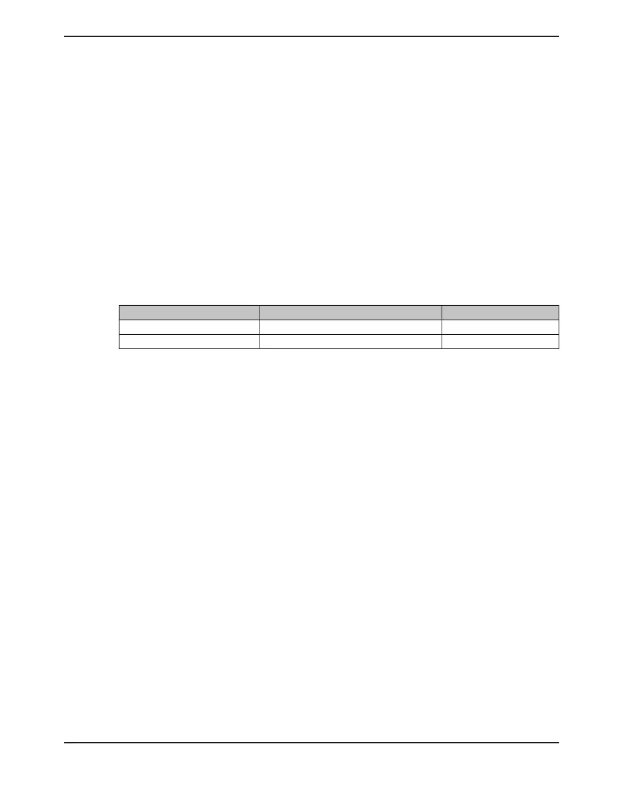
Deep-Sleep mode. The following table shows the maximum System Clock and PIOSC frequency
with respect to the LDO voltage.
Table 5-9. Maximum System Clock and PIOSC Frequency with Respect to LDO Voltage
PIOSCMaximum System Clock FrequencyOperating Voltage (LDO)
16 MHz120 MHz1.2
16 MHz30 MHz0.9
The LDO Power Calibration registers, LDOSPCAL and LDODPCAL, provide suggested values for
the LDO in the various modes. If software requests an LDO value that is too low or too high, the
value is not accepted and an error is reported in the SDPMST register.
Note: When using the USB, Ethernet, EPI, and QSSI interfaces, the LDO must be configured to
1.2 V.
Flash Memory and SRAM Power Control
During Sleep or Deep-Sleep mode, Flash memory can be in either the default active mode or the
low power mode; SRAM can be in the default active mode, standby mode, or low power mode. The
active mode in each case provides the fastest times to sleep and wake up, but consumes more
power. Low power mode provides the lowest power consumption, but takes longer to sleep and
wake up.
The SRAM can be programmed to prohibit any power management by configuring the SRAMPM bit
in the Sleep Power Configuration (SLPPWRCFG) register. This configuration operates in the
same way that legacy Stellaris
®
devices operate and provides the fastest sleep and wake-up times,
but consumes the most power while in Sleep and Deep-Sleep mode.
The following power saving options are available in Sleep and Deep-Sleep modes:
■ The clocks can be gated according to the settings in the peripheral-specific SCGC or DCGC
registers.
■ In Deep-Sleep mode, the clock source can be changed and the PIOSC can be powered off (if
no active peripheral requires it) using the DSCLKCFG register. These options are not available
for Sleep mode.
■ The LDO voltage can be changed using the LDOSPCTL or LDODPCTL register.
■ The Flash memory can be put into low power mode.
June 18, 2014244
Texas Instruments-Production Data
System Control
 Loading...


