Register 26: GPIO 12-mA Drive Select (GPIODR12R), offset 0x53C
The GPIODR12R register is the 12-mA drive control register. Each GPIO signal in the port can be
individually configured without affecting the other pads.
Note: This register has no effect on port pins PL6 and PL7 or PM[7:4].
GPIO 12-mA Drive Select (GPIODR12R)
GPIO Port A (AHB) base: 0x4005.8000
GPIO Port B (AHB) base: 0x4005.9000
GPIO Port C (AHB) base: 0x4005.A000
GPIO Port D (AHB) base: 0x4005.B000
GPIO Port E (AHB) base: 0x4005.C000
GPIO Port F (AHB) base: 0x4005.D000
GPIO Port G (AHB) base: 0x4005.E000
GPIO Port H (AHB) base: 0x4005.F000
GPIO Port J (AHB) base: 0x4006.0000
GPIO Port K (AHB) base: 0x4006.1000
GPIO Port L (AHB) base: 0x4006.2000
GPIO Port M (AHB) base: 0x4006.3000
GPIO Port N (AHB) base: 0x4006.4000
GPIO Port P (AHB) base: 0x4006.5000
GPIO Port Q (AHB) base: 0x4006.6000
Offset 0x53C
Type RW, reset 0x0000.0000
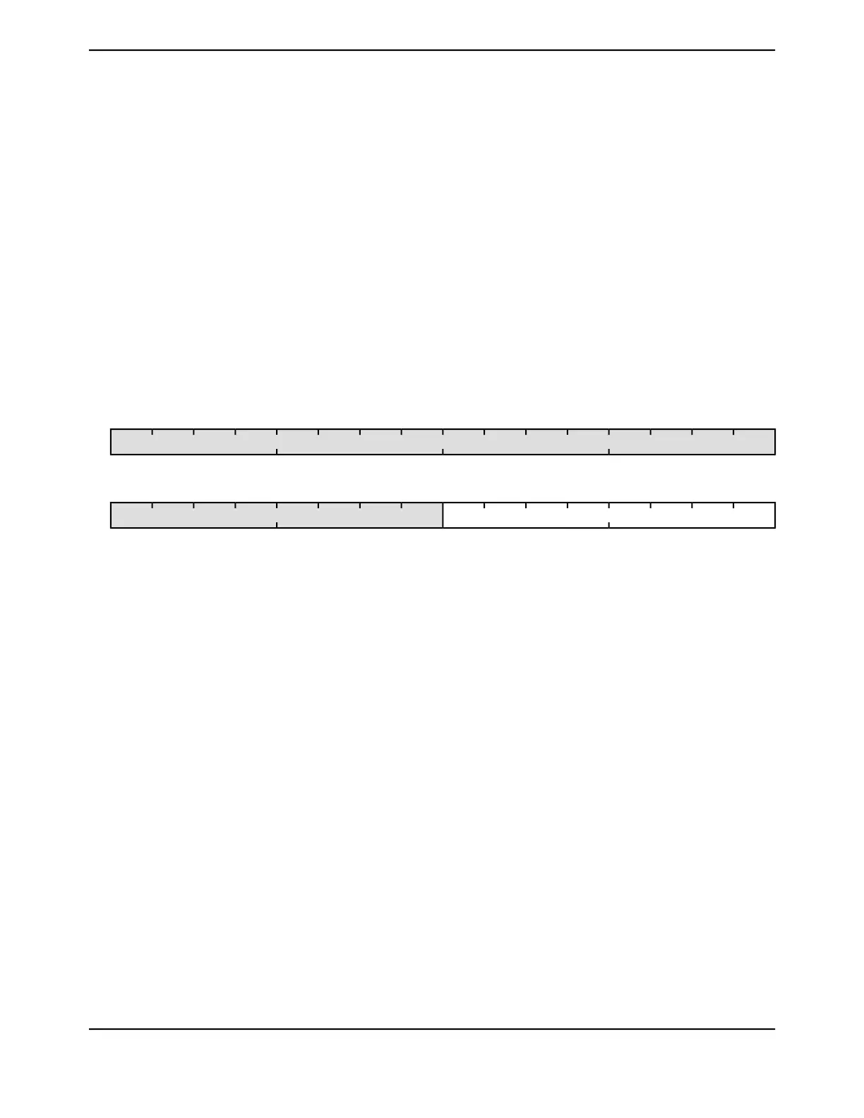
16171819202122232425262728293031
reserved
ROROROROROROROROROROROROROROROROType
0000000000000000Reset
0123456789101112131415
DRV12reserved
RWRWRWRWRWRWRWRWROROROROROROROROType
0000000000000000Reset
DescriptionResetTypeNameBit/Field
Software should not rely on the value of a reserved bit. To provide
compatibility with future products, the value of a reserved bit should be
preserved across a read-modify-write operation.
0x0000.00ROreserved31:8
Output Pad 12-mA Drive Enable
DescriptionValue
The drive for the corresponding GPIO pin is controlled by the
GPIODR2R, GPIODR4R, and/or the GPIODR8R register.
0
The corresponding GPIO pin has 12-mA drive. This encoding
is only valid if the GPIOPP EDE bit is set and the appropriate
GPIOPC EDM bit field is programmed to 0x3.
1
Note: Please refer to Table 10-3 on page 753 for information on how
to configure the drive strength.
Changes in the GPIODR2R, the GPIODR4R register and/or the
GPIODR8R registers to configure 12 mA are effective on the next clock
cycle.
0x00RWDRV127:0
June 18, 2014792
Texas Instruments-Production Data
General-Purpose Input/Outputs (GPIOs)
 Loading...


