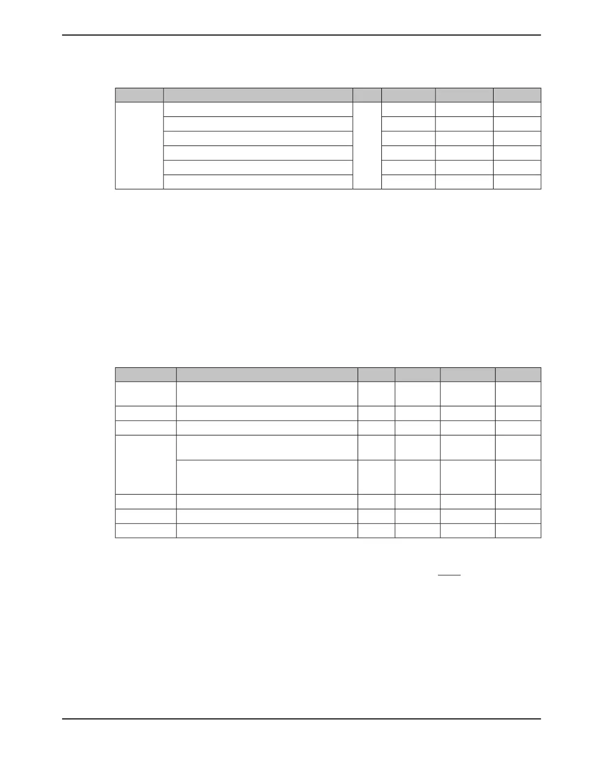
Table 27-34. Fast GPIO Module Characteristics (continued)
UnitMaxNomMinParameter NameParameter
ns16.510.3
-
Fast GPIO fall time, 2-mA drive
i
T
GPIOF
ns8.295.15Fast GPIO fall time, 4-mA drive
i
ns4.162.58Fast GPIO fall time, 8-mA drive
i
ns5.553.54Fast GPIO fall time, 8-mA drive with slew rate control
i
ns3.342.07Fast GPIO fall time, 10-mA drive
i
ns2.781.73Fast GPIO fall time, 12-mA drive
i
a. V
DD
must be within the range specified in Table 27-6 on page 1820.
b. Leakage and Injection current characteristics specified in this table also apply to XOSC0 and XOSC1 inputs.
c. Note that for the ADC's external reference inputs, care must be taken to avoid a current limiting resistor (refer to I
VREF
spec in Table 27-44 on page 1861)
d. I/O pads should be protected if at any point the IO voltage has a possibility of going outside the limits shown in the table.
If the part is unpowered, the IO pad Voltage or Current must be limited (as shown in this table) to avoid powering the
part through the IO pad, causing potential irreversible damage.
e. Refer to individual peripheral sections for specific loading information.
f. This value includes all GPIO except for port pins PL6 and PL7.
g. The leakage current is measured with V
IN
applied to the corresponding pin(s). The leakage of digital port pins is measured
individually. The port pin is configured as an input and the pull-up/pull-down resistor is disabled.
h. Time measured from 20% to 80% of V
DD
.
i. Time measured from 80% to 20% of V
DD
.
Table 27-35. Slow GPIO Module Characteristics
abc
UnitMaxNomMinParameter NameParameter
pF50--Capacitive loading for measurements given in this
table
d
C
LGPIO
kΩ31.420.013.8Slow GPIO internal pull-up resistorR
GPIOPU
kΩ35.520.513.0Slow GPIO internal pull-down resistorR
GPIOPD
nA3.25--Slow GPIO input leakage current, 0 V ≤ V
IN
≤ V
DD
GPIO pins
e
I
LKG+
nA3.25--Slow GPIO input leakage current, 0 V < V
IN
≤ V
DD
,
GPIO pins configured as ADC or analog comparator
inputs
µA3.42--DC injection current, V
IN
≤ 0 VI
INJ-
ns29.819.3-Slow GPIO rise time, 2-mA drive
f
T
GPIOR
ns21.112.8-Slow GPIO fall time, 2-mA drive
g
T
GPIOF
a. V
DD
must be within the range specified in Table 27-6 on page 1820.
b. V
IN
must be within the range specified in Table 27-1 on page 1818. Leakage current outside of this maximum voltage is not
guaranteed and can result in permanent damage of the device.
c. To avoid potential damage to the part, either the voltage or current on the non-Power, non-WAKE input/outputs should
be limited externally as shown in this table.
d. Refer to individual peripheral sections for specific loading information.
e. The leakage current is measured with V
IN
applied to the corresponding pin(s). The leakage of digital port pins is measured
individually. The port pin is configured as an input and the pull-up/pull-down resistor is disabled.
f. Time measured from 20% to 80% of V
DD
.
g. Time measured from 80% to 20% of V
DD
.
June 18, 20141850
Texas Instruments-Production Data
Electrical Characteristics
 Loading...


