controls the baud rate of CS2n and the COUNT1 bit field is programmed to control the baud rate of
CS3n.
Additionally, the Host-Bus mode provides read and write wait states for the data portion to support
different classes of device. These wait states stretch the data period (hold the rising edge of data
strobe) and may be used in all four sub-modes. The wait states are set using the WRWS and RDWS
bits in the EPI Host-Bus n Configuration (EPIHBnCFGn) register. The WRWS and RDWS bits are
enhanced with more precision by WRWSM and RDWSM bits in the EPIHBnTIMEn registers. Note none
of the wait state configuration bits can be set concurrently with the BURST bit in the same
EPIHBnCFGn register. See Table 11-11 on page 843 for programming information.
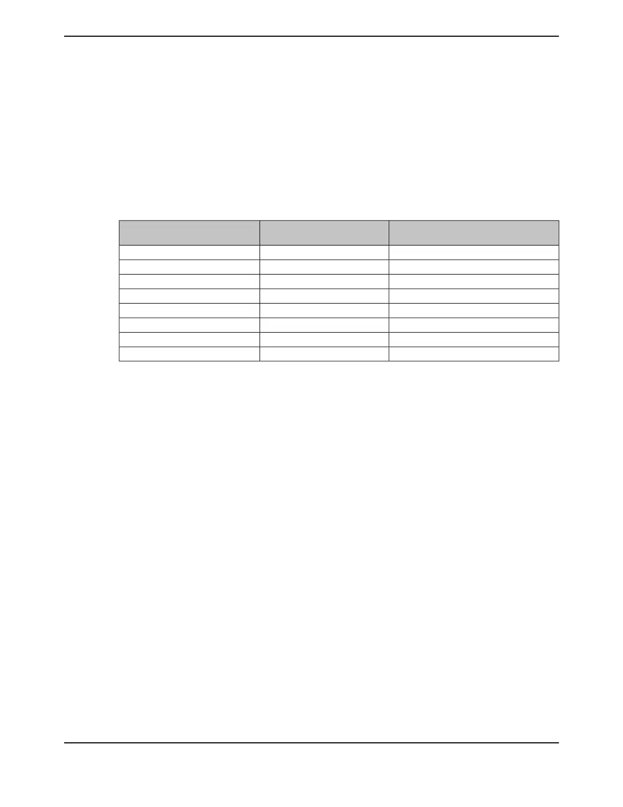
Table 11-11. Data Phase Wait State Programming
Data Phase Wait StatesRDWSM or WRWSM Encoding in
EPIHBnTIMEn Registers
RDWS or WRWS Encoding in
EPIHBnCFGn Register
1 EPI clocks10x0
2 EPI clocks00x0
3 EPI clocks10x1
4 EPI clocks00x1
5 EPI clocks10x2
6 EPI clocks00x2
7 EPI clocks10x3
8 EPI clocks00x3
The CAPWIDTH bit in EPIHBnTIMEn registers controls the delay between Host-Bus transfers. When
the CSBAUD bit is set and multi-chip selects have been configured in the EPIHBnCFG2 registers,
delay takes an additional clock cycle to adjust the clock rate of different chip selects.
Word read and write transactions can be enhanced through the enabling of the BURST bit in the
EPIHB16CFGn registers.
11.4.3.5 Sub-Modes of Host Bus 8/16
The EPI controller supports four variants of the Host-Bus model using 8 or 16 bits of data in all four
cases. The four sub-modes are selected using the MODE bits in the EPIHBnCFG register, and are:
1. Address and data are muxed. This scheme is used by many 8051 devices, some Microchip PIC
parts, and some ATmega parts. When used for standard SRAMs, a latch must be used between
the microcontroller and the SRAM. This sub-mode is provided for compatibility with existing
devices that support data transfers without a latch (that is, CPLDs). In general, the de-muxed
sub-mode should normally be used. The ALE configuration should be used in this mode, as all
Host-Bus accesses have an address phase followed by a data phase. The ALE indicates to an
external latch to capture the address then hold until the data phase. The ALE configuration is
controlled by configuring the CSCFG and CSCFGEXT field to be 0x0 in the EPIHBnCFG2 register.
The ALE can be enhanced to access two or four external devices with four separate CSn signals.
By configuring the CSCFG field to be 0x3 and the CSCFGEXT bit to be 0 in the EPIHBnCFG2
register, EPI0S30 functions as ALE, EPI0S27 functions as CS1n, and EPI0S26 functions as
CS0n. When the CSCFG field is set to 0x0 and the CSCFGEXT bit is set to 1 in the EPIHBnCFG2
register, EPI0S30 functions as ALE, EPIOS33 functions as CS3n, EPIOS34 functions as CS2n,
EPI0S27 functions as CS1n, and EPI0S26 functions as CS0n. The CSn is best used for
Host-Bus unmuxed mode, in which EPI address and data pins are separate. The CSn indicates
when the address and data phases of a read or write access are occurring.
843June 18, 2014
Texas Instruments-Production Data
Tiva
™
TM4C1294NCPDT Microcontroller
 Loading...


