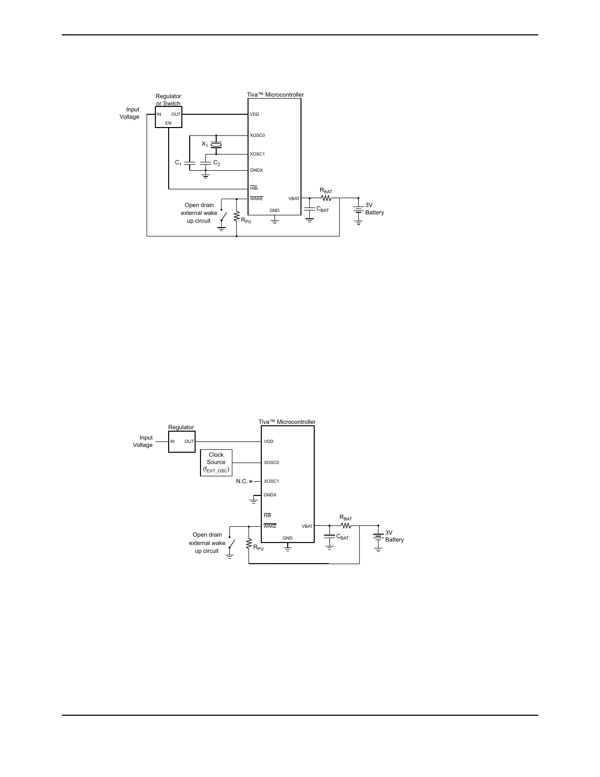
Figure 7-2. Using a Crystal as the Hibernation Clock Source with a Single Battery Source
Open drain
external wake
up circuit
3V
Battery
GND
C
2
C
1
X
1
VBAT
EN
Input
Voltage
Regulator
or Switch
XOSC1
XOSC0
VDD
HIB
WAKE
OUTIN
R
PU
GNDX
R
BAT
C
BAT
Tiva™ Microcontroller
Note: Some devices may not supply the GNDX signal. If GNDX is absent, the crystal load capacitors can
be tied to GND externally. See “Signal Tables” on page 1772 for pins specific to your device.
X
1
= Crystal frequency is f
XOSC_XTAL
.
C
1,2
= Capacitor value derived from crystal vendor load capacitance specifications.
R
PU
= Pull-up resistor is 200 kΩ
R
BAT
= 51Ω ±5%
C
BAT
= 0.1µF ±20%
See “Hibernation Clock Source Specifications” on page 1837 for specific parameter values.
Figure 7-3. Using a Dedicated Oscillator as the Hibernation Clock Source with VDD3ON Mode
Open drain
external wake
up circuit
GND
Input
Voltage
Regulator
Clock
Source
(f
EXT_OSC
)
N.C.
XOSC1
XOSC0
VDD
HIB
WAKE VBAT
OUT
IN
R
PU
GNDX
3V
Battery
R
BAT
C
BAT
Tiva™ Microcontroller
Note: Some devices may not supply a GNDX signal. See “Signal Tables” on page 1772 for pins specific to
your device.
R
PU
= Pull-up resistor is 1 MΩ
R
BAT
= 51Ω ±5%
C
BAT
= 0.1µF ±20%
537June 18, 2014
Texas Instruments-Production Data
Tiva
™
TM4C1294NCPDT Microcontroller
 Loading...


