15.3.2.6 Sample Phase Control
The trigger source for ADC0 and ADC1 may be independent or the two ADC modules may operate
from the same trigger source and operate on the same or different inputs. If the converters are
running at the same sample rate, they may be configured to start the conversions coincidentally or
one ADC may be programmed to lag up to 15 clock cycles relative to the other ADC. The sample
time can be delayed from the standard sampling time by programming the PHASE field in the ADC
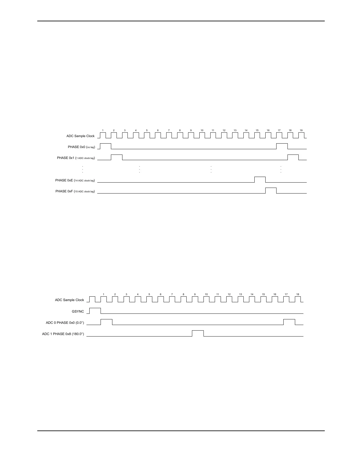
Sample Phase Control (ADCSPC) register. Figure 15-3 on page 1060 shows an example of various
phase relationships.
Figure 15-3. ADC Sample Phases
1 2 3 4 5 6 7 8 9 10 11 12 13 14 15 16 17 18
ADC Sample Clock
PHASE 0x0 (no lag)
PHASE 0x1 (1 ADC clock lag)
PHASE 0xE (14 ADC clock lag)
PHASE 0xF (15 ADC clock lag)
.
.
.
.
.
.
.
.
.
.
.
.
19
This feature can be used to double the sampling rate of an input. Both ADC Module 0 and ADC
Module 1 can be programmed to sample the same input. ADC module 0 can sample at the standard
position (the PHASE field in the ADCSPC register is 0x0). ADC Module 1 can be configured to sample
with a phase lag (PHASE is nonzero). For a sample rate of two million samples/second at 16MHz,
the TSHn field of all of the sequencer samples of both ADCs must be programmed to 0x0 and the
PHASE field of one of the ADC modules must be set to 0x8. The two modules can be be synchronized
using the GSYNC and SYNCWAIT bits in the ADC Processor Sample Sequence Initiate (ADCPSSI)
register. Software can then combine the results from the two modules to create a sample rate of
two million samples/second at 16MHz as shown in Figure 15-4 on page 1060.
Figure 15-4. Doubling the ADC Sample Rate
1 2 3 4 5 6 7 8 9 10 11 12 13 14 15 16 17
ADC Sample Clock
GSYNC
ADC 0 PHASE 0x0 (0.0°)
ADC 1 PHASE 0x8 (180.0°)
18
Using the ADCSPC register, ADC0 and ADC1 may provide a number of interesting applications:
■ Coincident continuous sampling of different signals. The sample sequence steps run coincidently
in both converters. In this situation, the TSHn of matching sample steps of both ADC module
sequencers must be the same and the PHASE field must be 0x0 in both ADC module ADCSPC
registers. The TSHn field is found in the ADC Sample Sequence n Sample and Hold Time
(ADCSSTSHn) register.
– ADC Module 0, ADCSPC = 0x0, sampling AIN0
June 18, 20141060
Texas Instruments-Production Data
Analog-to-Digital Converter (ADC)
 Loading...


