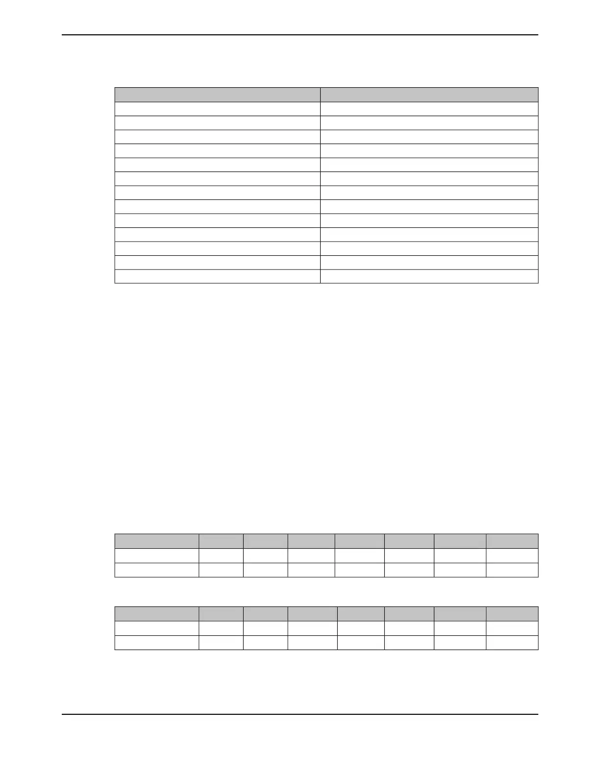
Table 15-3. Sample and Hold Width in ADC Clocks (continued)
N
SH
TSHn Encoding
reserved0x1
80x2
reserved0x3
160x4
reserved0x5
320x6
reserved0x7
640x8
reserved0x9
1280xA
reserved0xB
2560xC
reserved0xD-0xF
The ADC conversion frequency is a function of the Sample and Hold number, given by the following
equation:
F
CONV
= 1/((N
SH
+ 12)*T
ADC
)
where:
■ N
SH
is the sample and hold width in ADC clocks
■ T
ADC
is the ADC conversion clock period, which is the inverse of the ADC clock frequency F
ADC
Now, the maximum allowable external source resistance (R
S
) also changes with the value of N
SH
,
as the total settling time of the input circuitry must be fast enough to settle to within the ADC resolution
in a single sampling interval. The input circuitry includes the external source resistance as well as
the input resistance and capacitance of the ADC (R
ADC
and C
ADC
).
The values for R
S
and F
CONV
for varying N
SH
values, with F
ADC
=16MHz and F
ADC
=32MHz are given
in tables 18-4-a and 18-4-b. The system designer must take into consideration both of these factors
for optimal ADC operation.
Table 15-4. R
S
and F
CONV
Values with Varying N
SH
Values and F
ADC
= 16 MHz
25612864321684N
SH
(Cycles)
601142113645718001000F
CONV
(Ksps)
18950093500455002150095003500500R
S
Max (Ω)
Table 15-5. R
S
and F
CONV
Values with Varying N
SH
Values and F
ADC
= 32 MHz
25612864321684N
SH
(Cycles)
119229421727114316002000F
CONV
(Ksps)
93500455002150095003500500250R
S
Max (Ω)
1059June 18, 2014
Texas Instruments-Production Data
Tiva
™
TM4C1294NCPDT Microcontroller
 Loading...


