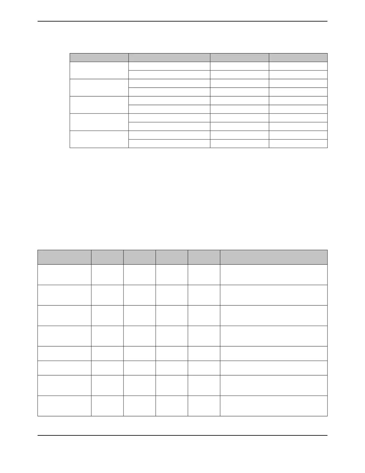
Table 13-1. Available CCP Pins (continued)
Odd CCP PinEven CCP PinUp/Down CounterTimer
-T3CCP0Timer A
16/32-Bit Timer 3
T3CCP1-Timer B
-T4CCP0Timer A
16/32-Bit Timer 4
T4CCP1-Timer B
-T5CCP0Timer A
16/32-Bit Timer 5
T5CCP1-Timer B
-T6CCP0Timer A
16/32-Bit Timer 6
T6CCP1-Timer B
-T7CCP0Timer A
16/32-Bit Timer 7
T7CCP1-Timer B
13.2 Signal Description
The following table lists the external signals of the GP Timer module and describes the function of
each. The GP Timer signals are alternate functions for some GPIO signals and default to be GPIO
signals at reset. The column in the table below titled "Pin Mux/Pin Assignment" lists the possible
GPIO pin placements for these GP Timer signals. The AFSEL bit in the GPIO Alternate Function
Select (GPIOAFSEL) register (page 770) should be set to choose the GP Timer function. The number
in parentheses is the encoding that must be programmed into the PMCn field in the GPIO Port
Control (GPIOPCTL) register (page 787) to assign the GP Timer signal to the specified GPIO port
pin. For more information on configuring GPIOs, see “General-Purpose Input/Outputs
(GPIOs)” on page 742.
Table 13-2. General-Purpose Timers Signals (128TQFP)
DescriptionBuffer TypePin TypePin Mux / Pin
Assignment
Pin NumberPin Name
16/32-Bit Timer 0 Capture/Compare/PWM 0.TTLI/OPD0 (3)
PA0 (3)
PL4 (3)
1
33
85
T0CCP0
16/32-Bit Timer 0 Capture/Compare/PWM 1.TTLI/OPD1 (3)
PA1 (3)
PL5 (3)
2
34
86
T0CCP1
16/32-Bit Timer 1 Capture/Compare/PWM 0.TTLI/OPD2 (3)
PA2 (3)
PL6 (3)
3
35
94
T1CCP0
16/32-Bit Timer 1 Capture/Compare/PWM 1.TTLI/OPD3 (3)
PA3 (3)
PL7 (3)
4
36
93
T1CCP1
16/32-Bit Timer 2 Capture/Compare/PWM 0.TTLI/OPA4 (3)
PM0 (3)
37
78
T2CCP0
16/32-Bit Timer 2 Capture/Compare/PWM 1.TTLI/OPA5 (3)
PM1 (3)
38
77
T2CCP1
16/32-Bit Timer 3 Capture/Compare/PWM 0.TTLI/OPA6 (3)
PM2 (3)
PD4 (3)
40
76
125
T3CCP0
16/32-Bit Timer 3 Capture/Compare/PWM 1.TTLI/OPA7 (3)
PM3 (3)
PD5 (3)
41
75
126
T3CCP1
957June 18, 2014
Texas Instruments-Production Data
Tiva
™
TM4C1294NCPDT Microcontroller
 Loading...


