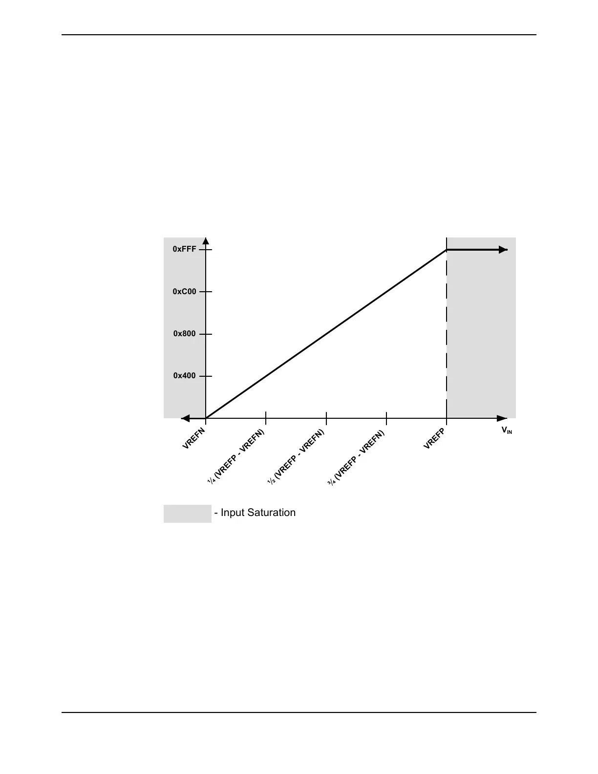
The range of this conversion value is from 0x000 to 0xFFF. In single-ended-input mode, the 0x000
value corresponds to the voltage level on VREFN; the 0xFFF value corresponds to the voltage level
on VREFP. This configuration results in a resolution that can be calculated using the following
equation:
mV per ADC code = (VREFP - VREFN) / 4096
While the analog input pads can handle voltages beyond this range, the analog input voltages must
remain within the limits prescribed by Table 27-44 on page 1861 to produce accurate results. The
V
REFA+
specification defines the useful range for the external voltage reference on VREFA+ and
GNDA, see Table 27-44 on page 1861. Care must be taken to supply a reference voltage of acceptable
quality.Figure 15-9 on page 1065 shows the ADC conversion function of the analog inputs.
Figure 15-9. ADC Conversion Result
0xFFF
V
IN
0xC00
0x800
0x400
VREFN
VREFP
½ (VREFP - VREFN)
¼ (VREFP - VREFN)
¾ (VREFP - VREFN)
- Input Saturation
15.3.5 Differential Sampling
In addition to traditional single-ended sampling, the ADC module supports differential sampling of
two analog input channels. To enable differential sampling, software must set the Dn bit in the
ADCSSCTL0n register in a step's configuration nibble.
When a sequence step is configured for differential sampling, the input pair to sample must be
configured in the ADCSSMUXn register. Differential pair 0 samples analog inputs 0 and 1; differential
1065June 18, 2014
Texas Instruments-Production Data
Tiva
™
TM4C1294NCPDT Microcontroller
 Loading...


