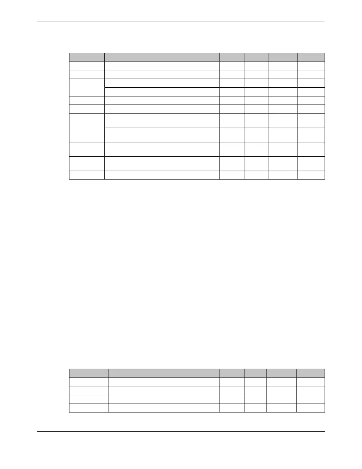
Table 27-22. Hibernation External Oscillator (XOSC) Input Characteristics (continued)
UnitMaxNomMinParameter NameParameter
pF-0.5-PCB stray shunt capacitance
b
C
PCB
pF4--Total shunt capacitance
b
C
SHUNT
kΩ50--Crystal effective series resistance, OSCDRV = 0
c
ESR
kΩ75--Crystal effective series resistance, OSCDRV = 1
c
µW0.25--Oscillator output drive levelDL
ms1500
e
600-Oscillator startup time, when using a crystal
d
T
START
V--2.64CMOS input high level, when using an external
oscillator with Supply > 3.3 V
V
IH
f
V--0.8 *
Supply
CMOS input high level, when using an external
oscillator with 1.8 V ≤ Supply ≤ 3.3 V
V0.2 * Supply--CMOS input low level, when using an external oscillator
with 1.8 V ≤ Supply ≤ 3.63 V
V
IL
f
mV1390960360CMOS input buffer hysteresis, when using an external
oscillator with 1.8 V ≤ Supply ≤ 3.63 V
V
HYS
f
%70-30External single-Ended (Bypass) reference duty cycleDC
HIBOSC_EXT
a. The HIB XOSC pins are non-failsafe and must follow the limits detailed in “Non-Power I/O Pins” on page 1851.
b. See information below table.
c. Crystal ESR specified by crystal manufacturer.
d. Oscillator startup time is specified from the time the oscillator is enabled to when it reaches a stable point of oscillation
such that the internal clock is valid.
e. Only valid for recommended supply conditions. Measured with OSCDRV bit set (high drive strength enabled, 24 pF).
f. Specification is relative to the larger of V
DD
or V
BAT
.
The load capacitors added on the board, C
1
and C
2
, should be chosen such that the following
equation is satisfied (see Table 27-22 on page 1837 for typical values).
■ C
L
= load capacitance specified by crystal manufacturer
■ C
L
= (C
1
*C
2
)/(C
1
+C
2
) + C
PKG
+ C
PCB
■ C
SHUNT
= C
PKG
+ C
PCB
+ C
0
(total shunt capacitance seen across XOSC0, XOSC1)
■ C
PKG
, C
PCB
as measured across the XOSC0, XOSC1 pins excluding the crystal
■ Clear the OSCDRV bit in the Hibernation Control (HIBCTL) register for C
1,2
≤ 18 pF; set the
OSCDRV bit for C
1,2
> 18 pF.
■ C
0
= Shunt capacitance of crystal specified by the crystal manufacturer
27.9.5 Main Oscillator Specifications
Table 27-23. Main Oscillator Input Characteristics
a
UnitMaxNomMinParameter NameParameter
MHz25-4
b
Parallel resonance frequencyF
MOSC
MHz120-0External clock reference (PLL in BYPASS mode)F
REF_XTAL_BYPASS
pF24-12External load capacitance on OSC0, OSC1 pins
c
C
1
, C
2
pF-0.5-Device package stray shunt capacitance
c
C
PKG
June 18, 20141838
Texas Instruments-Production Data
Electrical Characteristics
 Loading...


