Register 1: GPIO Data (GPIODATA), offset 0x000
The GPIODATA register is the data register. In software control mode, values written in the
GPIODATA register are transferred onto the GPIO port pins if the respective pins have been
configured as outputs through the GPIO Direction (GPIODIR) register (see page 760).
In order to write to GPIODATA, the corresponding bits in the mask, resulting from the address bus
bits [9:2], must be set. Otherwise, the bit values remain unchanged by the write.
Similarly, the values read from this register are determined for each bit by the mask bit derived from
the address used to access the data register, bits [9:2]. Bits that are set in the address mask cause
the corresponding bits in GPIODATA to be read, and bits that are clear in the address mask cause
the corresponding bits in GPIODATA to be read as 0, regardless of their value.
A read from GPIODATA returns the last bit value written if the respective pins are configured as
outputs, or it returns the value on the corresponding input pin when these are configured as inputs.
All bits are cleared by a reset.
GPIO Data (GPIODATA)
GPIO Port A (AHB) base: 0x4005.8000
GPIO Port B (AHB) base: 0x4005.9000
GPIO Port C (AHB) base: 0x4005.A000
GPIO Port D (AHB) base: 0x4005.B000
GPIO Port E (AHB) base: 0x4005.C000
GPIO Port F (AHB) base: 0x4005.D000
GPIO Port G (AHB) base: 0x4005.E000
GPIO Port H (AHB) base: 0x4005.F000
GPIO Port J (AHB) base: 0x4006.0000
GPIO Port K (AHB) base: 0x4006.1000
GPIO Port L (AHB) base: 0x4006.2000
GPIO Port M (AHB) base: 0x4006.3000
GPIO Port N (AHB) base: 0x4006.4000
GPIO Port P (AHB) base: 0x4006.5000
GPIO Port Q (AHB) base: 0x4006.6000
Offset 0x000
Type RW, reset 0x0000.0000
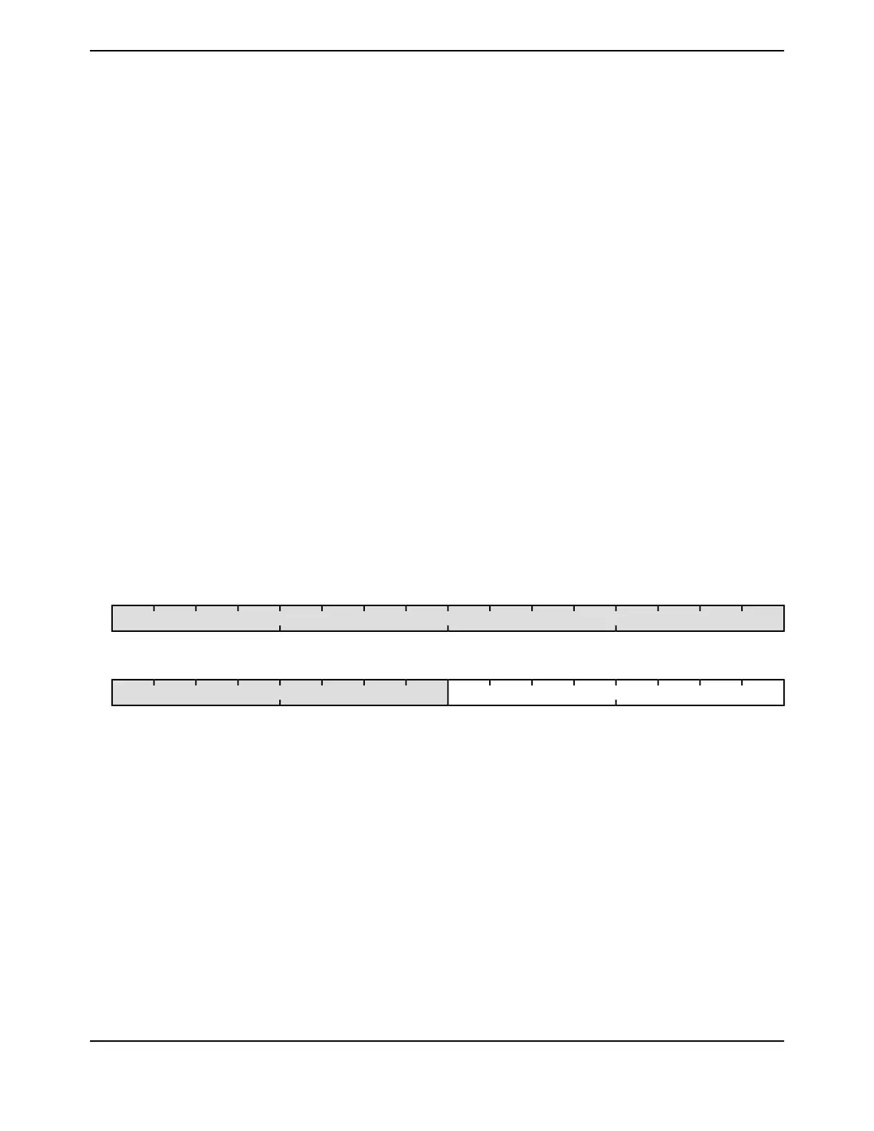
16171819202122232425262728293031
reserved
ROROROROROROROROROROROROROROROROType
0000000000000000Reset
0123456789101112131415
DATAreserved
RWRWRWRWRWRWRWRWROROROROROROROROType
0000000000000000Reset
DescriptionResetTypeNameBit/Field
Software should not rely on the value of a reserved bit. To provide
compatibility with future products, the value of a reserved bit should be
preserved across a read-modify-write operation.
0x0000.00ROreserved31:8
GPIO Data
This register is virtually mapped to 256 locations in the address space.
To facilitate the reading and writing of data to these registers by
independent drivers, the data read from and written to the registers are
masked by the eight address lines [9:2]. Reads from this register return
its current state. Writes to this register only affect bits that are not masked
by ADDR[9:2] and are configured as outputs. See “Data Register
Operation” on page 749 for examples of reads and writes.
0x00RWDATA7:0
759June 18, 2014
Texas Instruments-Production Data
Tiva
™
TM4C1294NCPDT Microcontroller
 Loading...


