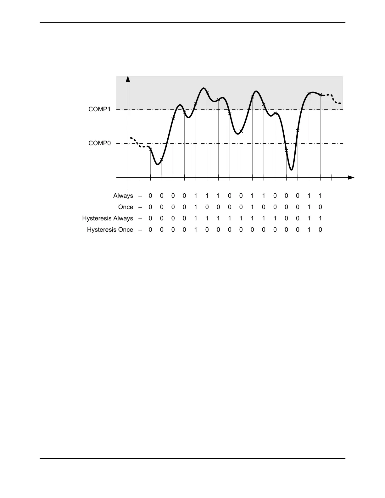
Figure 15-14. High-Band Operation (CIC=0x3 and/or CTC=0x3)
0
0
0
0
0
0
0
0
0
0
0
0
0
0
0
0
1
1
1
1
1
0
1
0
1
0
1
0
0
0
1
0
0
0
1
0
1
1
1
0
1
0
1
0
0
0
1
0
0
0
0
0
0
0
0
0
1
1
1
1
1
0
1
0
Always –
Once –
Hysteresis Always –
Hysteresis Once –
COMP0
COMP1
15.4 Initialization and Configuration
15.4.1 Module Initialization
Initialization of the ADC module is a simple process with very few steps: enabling the clock to the
ADC, disabling the analog isolation circuit associated with all inputs that are to be used, and
reconfiguring the sample sequencer priorities (if needed).
The initialization sequence for the ADC is as follows:
1. Enable the ADC clock using the RCGCADC register (see page 396).
2. Enable the clock to the appropriate GPIO modules via the RCGCGPIO register (see page 382).
To find out which GPIO ports to enable, refer to “Signal Description” on page 1055.
3. Set the GPIO AFSEL bits for the ADC input pins (see page 770). To determine which GPIOs to
configure, see Table 26-4 on page 1797.
4. Configure the AINx signals to be analog inputs by clearing the corresponding DEN bit in the
GPIO Digital Enable (GPIODEN) register (see page 781).
5. Disable the analog isolation circuit for all ADC input pins that are to be used by writing a 1 to
the appropriate bits of the GPIOAMSEL register (see page 786) in the associated GPIO block.
6. If required by the application, reconfigure the sample sequencer priorities in the ADCSSPRI
register. The default configuration has Sample Sequencer 0 with the highest priority and Sample
Sequencer 3 as the lowest priority.
June 18, 20141072
Texas Instruments-Production Data
Analog-to-Digital Converter (ADC)
 Loading...


