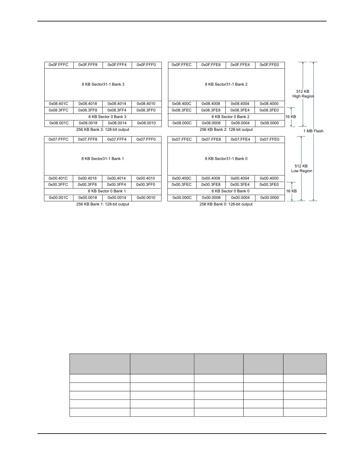
Figure 8-2. Flash Memory Configuration
0x0F.FFFC 0x0F.FFF8 0x0F.FFF4 0x0F.FFF0
0x08.3FFC 0x08.3FF8 0x08.3FF4 0x08.3FF0
0x08.401C 0x08.4018 0x08.4014 0x08.4010
0x08.001C 0x08.0018 0x08.0014 0x08.0010
8 KB Sector 0 Bank 3
8 KB Sector31-1 Bank 3
0x0F.FFEC 0x0F.FFE8 0x0F.FFE4 0x0F.FFE0
0x08.3FEC 0x08.3FE8 0x08.3FE4 0x08.3FE0
0x08.400C 0x08.4008 0x08.4004 0x08.4000
0x08.000C 0x08.0008 0x08.0004 0x08.0000
8 KB Sector 0 Bank 2
8 KB Sector31-1 Bank 2
0x07.FFFC 0x07.FFF8 0x07.FFF4 0x07.FFF0
0x00.3FFC 0x00.3FF8 0x00.3FF4 0x00.3FF0
0x00.401C 0x00.4018 0x00.4014 0x00.4010
0x00.001C 0x00.0018 0x00.0014 0x00.0010
8 KB Sector 0 Bank 1
8 KB Sector31-1 Bank 1
0x07.FFEC 0x07.FFE8 0x07.FFE4 0x07.FFE0
0x00.3FEC 0x00.3FE8 0x00.3FE4 0x00.3FE0
0x00.400C 0x00.4008 0x00.4004 0x00.4000
0x00.000C 0x00.0008 0x00.0004 0x00.0000
8 KB Sector 0 Bank 0
8 KB Sector31-1 Bank 0
256 KB Bank 1: 128-bit output 256 KB Bank 0: 128-bit output
256 KB Bank 2: 128-bit output256 KB Bank 3: 128-bit output
16 KB
16 KB
512 KB
High Region
512 KB
Low Region
1 MB Flash
The interleaved memory prefetchs 256 bits at a time. The prefetch buffers allow the maximum
performance of a 120 MHz CPU speed to be maintained with linear code or loops that fit within the
prefetch buffer. It is recommended that code be compiled with switches set to eliminate "literals" as
much as possible as a literal causes a flash access for that word and a stall for the wait states. Most
compilers support transforming literals into "in-line" code, which executes faster in a system where
the memory subsystem is slower than the CPU.
Because the memory is two-way interleaved and each bank individually is an 8-KB sector, when
the user erases a sector, using the ERASE bits in the Flash Memory Control (FMC) register, it is
a 16 KB erase. Erasing a block causes the entire contents of the block to be reset to all 1s.
8.2.3.1 Flash Configuration
Depending on the CPU frequency, the application must program the Flash clock high time (FBCHT),
Flash Bank Clock Edge (FBCE) and Flash wait states (FWS) in the Memory Timing Parameter
Register 0 for Main Flash and EEPROM (MEMTIM0), System Control Module offset 0x0C0. The
following table details the bit field values that are required for the given CPU frequency ranges.
Table 8-1. MEMTIM0 Register Configuration versus Frequency
Flash Wait States
(FWS)
Flash Bank
Clock Edge
(FBCE)
Flash Bank Clock
High Time (FBCHT)
Time Period Range (t) in nsCPU Frequency range (f)
in MHz
0x010x062.516
0x100x262.5 > t ≥ 2516 < f ≤ 40
0x200x325 > t ≥ 16.6740 < f ≤60
0x300x416.67 > t ≥ 12.560< f ≤80
0x400x512.5 > t ≥ 1080 < f ≤100
605June 18, 2014
Texas Instruments-Production Data
Tiva
™
TM4C1294NCPDT Microcontroller
 Loading...


