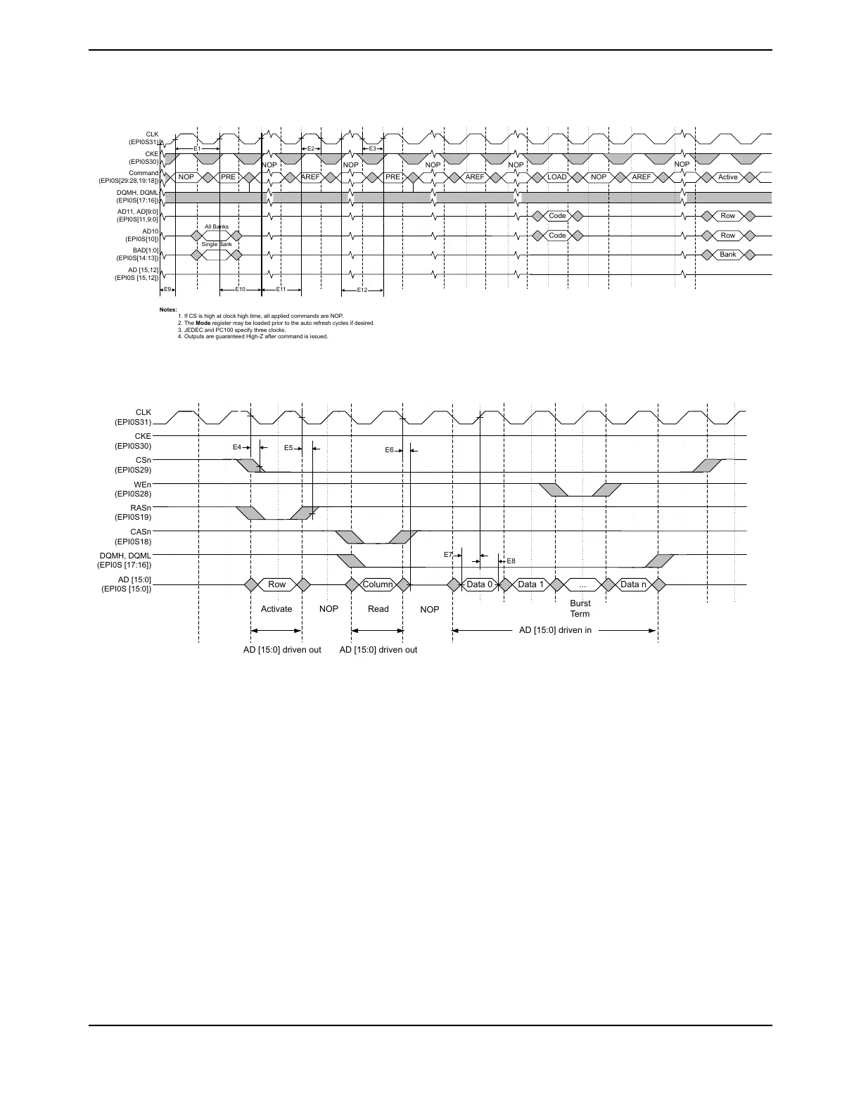
Figure 27-18. SDRAM Initialization and Load Mode Register Timing
CLK
(EPI0S31)
CKE
(EPI0S30)
Command
(EPI0S[29:28,19:18])
DQMH, DQML
(EPI0S[17:16])
AD11, AD[9:0]
(EPI0S[11,9:0]
AD10
(EPI0S[10])
BAD[1:0]
(EPI0S[14:13])
AD [15,12]
(EPI0S [15,12])
NOP
PRE
NOP
AREF
NOP
PRE
NOP
AREF
NOP
LOAD
Code
All Banks
Single Bank
Code
Notes:
1. If CS is high at clock high time, all applied commands are NOP.
2. The Mode register may be loaded prior to the auto refresh cycles if desired.
3. JEDEC and PC100 specify three clocks.
4. Outputs are guaranteed High-Z after command is issued.
E9
E10 E11
E12
E1 E2
E3
NOP
AREF
NOP
Active
Row
Row
Bank
Figure 27-19. SDRAM Read Timing
Row Column Data 0 Data 1 ... Data n
CLK
(EPI0S31)
CKE
(EPI0S30)
CSn
(EPI0S29)
WEn
(EPI0S28)
RASn
(EPI0S19)
CASn
(EPI0S18)
DQMH, DQML
(EPI0S [17:16])
AD [15:0]
(EPI0S [15:0])
Activate NOP Read
NOP
Burst
Term
AD [15:0] driven in
AD [15:0] driven out AD [15:0] driven out
E4
E5
E6
E7
E8
June 18, 20141854
Texas Instruments-Production Data
Electrical Characteristics
 Loading...


