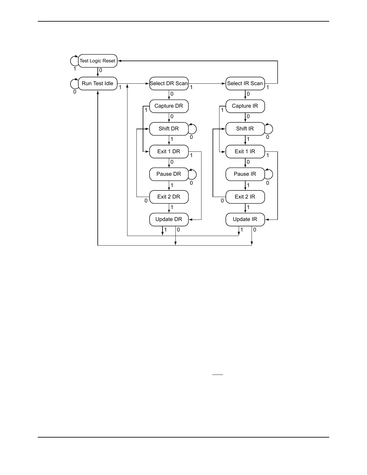
Figure 4-2. Test Access Port State Machine
Test Logic Reset
Run Test Idle Select DR Scan Select IR Scan
Capture DR Capture IR
Shift DR Shift IR
Exit 1 DR Exit 1 IR
Exit 2 DR Exit 2 IR
Pause DR Pause IR
Update DR Update IR
1 11
1 1
1
1 1
1 1
1 1
1 1
1 10 0
00
00
0 0
0 0
0 0
00
0
0
4.3.3 Shift Registers
The Shift Registers consist of a serial shift register chain and a parallel load register. The serial shift
register chain samples specific information during the TAP controller's CAPTURE states and allows
this information to be shifted out on TDO during the TAP controller's SHIFT states. While the sampled
data is being shifted out of the chain on TDO, new data is being shifted into the serial shift register
on TDI. This new data is stored in the parallel load register during the TAP controller's UPDATE
states. Each of the shift registers is discussed in detail in “Register Descriptions” on page 215.
4.3.4 Operational Considerations
Certain operational parameters must be considered when using the JTAG module. Because the
JTAG pins can be programmed to be GPIOs, board configuration and reset conditions on these
pins must be considered. In addition, because the JTAG module has integrated ARM Serial Wire
Debug, the method for switching between these two operational modes is described below.
4.3.4.1 GPIO Functionality
When the microcontroller is reset with either a POR or RST, the JTAG/SWD port pins default to their
JTAG/SWD configurations. The default configuration includes enabling digital functionality (DEN[3:0]
set in the Port C GPIO Digital Enable (GPIODEN) register), enabling the pull-up resistors (PUE[3:0]
set in the Port C GPIO Pull-Up Select (GPIOPUR) register), disabling the pull-down resistors
(PDE[3:0] cleared in the Port C GPIO Pull-Down Select (GPIOPDR) register) and enabling the
June 18, 2014212
Texas Instruments-Production Data
JTAG Interface
 Loading...


