■ GPIO Port J (AHB): 0x4006.0000
■ GPIO Port K (AHB): 0x4006.1000
■ GPIO Port L (AHB): 0x4006.2000
■ GPIO Port M (AHB): 0x4006.3000
■ GPIO Port N (AHB): 0x4006.4000
■ GPIO Port P (AHB): 0x4006.5000
■ GPIO Port Q (AHB): 0x4006.6000
Note that each GPIO module clock must be enabled before the registers can be programmed (see
page 382). There must be a delay of 3 system clocks after the GPIO module clock is enabled before
any GPIO module registers are accessed.
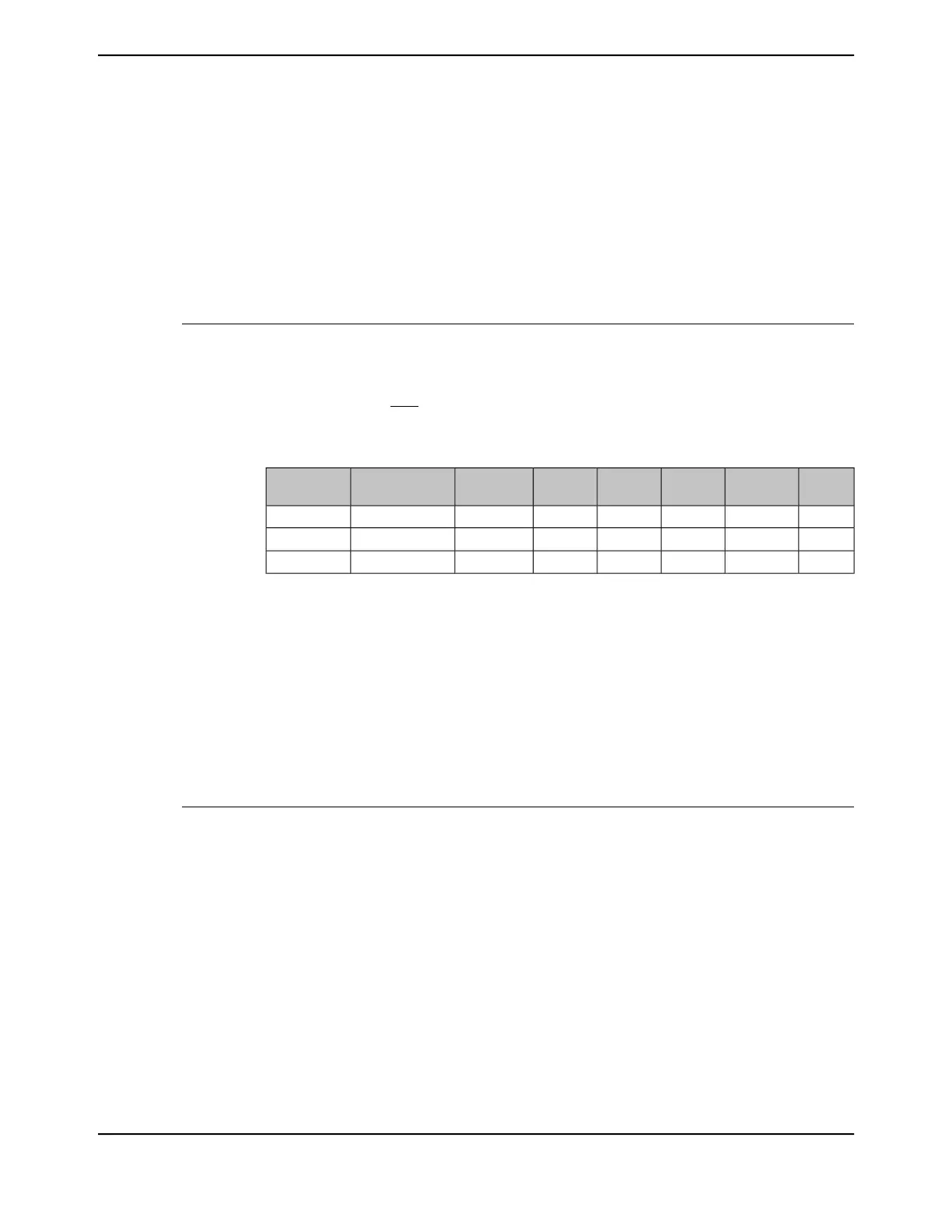
Important: The table below shows special consideration GPIO pins. Most GPIO pins are configured
as GPIOs and tri-stated by default (GPIOAFSEL=0, GPIODEN=0, GPIOPDR=0,
GPIOPUR=0, and GPIOPCTL=0). Special consideration pins may be programed to a
non-GPIO function or may have special commit controls out of reset. In addition, a
Power-On-Reset (POR) returns these GPIO to their original special consideration state.
Table 10-6. GPIO Pins With Special Considerations
GPIOCRGPIOPCTLGPIOPURGPIOPDRGPIODENGPIOAFSELDefault Reset
State
GPIO Pins
00x11011JTAG/SWDPC[3:0]
00x00000GPIO
a
PD[7]
00x00000GPIO
a
PE[7]
a. This pin is configured as a GPIO by default but is locked and can only be reprogrammed by unlocking the
pin in the GPIOLOCK register and uncommitting it by setting the GPIOCR register.
The GPIO commit control registers provide a layer of protection against accidental
programming of critical hardware signals including the GPIO pins that can function as
JTAG/SWD signals and the NMI signal. The commit control process must be followed
for these pins, even if they are programmed as alternate functions other than JTAG/SWD
or NMI; see “Commit Control” on page 752.
Note: If the device fails initialization during reset, the hardware toggles the TDO output
as an indication of failure. Thus, during board layout, designers should not
designate the TDO pin as a GPIO in sensitive applications where the possibility
of toggling could affect the design.
The default register type for the GPIOCR register is RO for all GPIO pins with the exception of the
NMI pin and the four JTAG/SWD pins (see “Signal Tables” on page 1772 for pin numbers). These six
pins are the only GPIOs that are protected by the GPIOCR register. Because of this, the register
type for the corresponding GPIO Ports is RW.
The default reset value for the GPIOCR register is 0x0000.00FF for all GPIO pins, with the exception
of the NMI and JTAG/SWD pins (see “Signal Tables” on page 1772 for pin numbers). To ensure that
the JTAG and NMI pins are not accidentally programmed as GPIO pins, these pins default to
non-committable. Because of this, the default reset value of GPIOCR changes for the corresponding
ports.
June 18, 2014756
Texas Instruments-Production Data
General-Purpose Input/Outputs (GPIOs)
 Loading...


