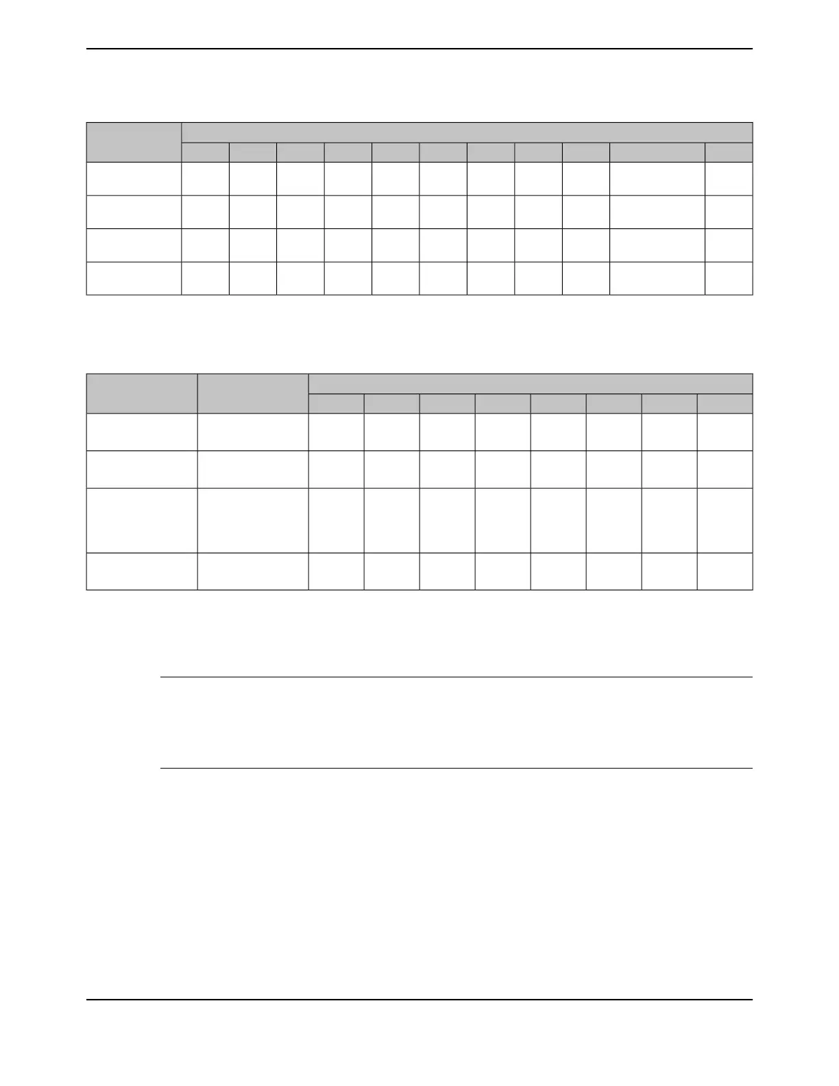
Table 10-4. GPIO Pad Configuration Examples (continued)
GPIO Register Bit Value
a
Configuration
SLRDR12RDR8RDR4RDR2RPDRPURDENODRDIRAFSEL
???????10X1Digital Input/Output
(SSI)
???????10X1Digital Input/Output
(UART)
XXXXX000000Analog Input
(Comparator)
???????10X1Digital Output
(Comparator)
a. X=Ignored (don’t care bit)
?=Can be either 0 or 1, depending on the configuration
Table 10-5. GPIO Interrupt Configuration Example
Pin 2 Bit Value
a
Desired Interrupt
Event Trigger
Register
01234567
XX0XXXXX0=edge
1=level
GPIOIS
XX0XXXXX0=single edge
1=both edges
GPIOIBE
XX1XXXXX0=Low level, or falling
edge
1=High level, or rising
edge
GPIOIEV
001000000=masked
1=not masked
GPIOIM
a. X=Ignored (don’t care bit)
10.5 Register Map
Table 10-7 on page 757 lists the GPIO registers.
Important: The GPIO registers in this chapter are duplicated in each GPIO block; however,
depending on the block, all eight bits may not be connected to a GPIO pad. In those
cases, writing to unconnected bits has no effect, and reading unconnected bits returns
no meaningful data. See “Signal Description” on page 743 for the GPIOs included on
this device.
The offset listed is a hexadecimal increment to the register's address, relative to that GPIO port's
base address:
■ GPIO Port A (AHB): 0x4005.8000
■ GPIO Port B (AHB): 0x4005.9000
■ GPIO Port C (AHB): 0x4005.A000
■ GPIO Port D (AHB): 0x4005.B000
■ GPIO Port E (AHB): 0x4005.C000
■ GPIO Port F (AHB): 0x4005.D000
■ GPIO Port G (AHB): 0x4005.E000
■ GPIO Port H (AHB): 0x4005.F000
755June 18, 2014
Texas Instruments-Production Data
Tiva
™
TM4C1294NCPDT Microcontroller
 Loading...


