Table 26-2. Signals by Pin Number (continued)
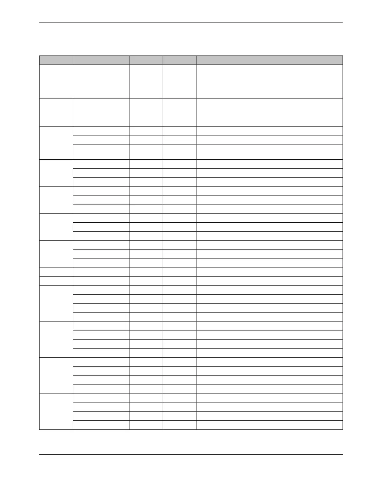
DescriptionBuffer TypePin TypePin NamePin Number
A reference voltage used to specify the voltage at which the ADC
converts to a maximum value. This pin is used in conjunction with
GNDA. The voltage that is applied to VREFA+ is the voltage with
which an AINn signal is converted to 4095. The VREFA+ voltage
is limited to the range specified in Table 27-44 on page 1861.
Analog-VREFA+
9
The ground reference for the analog circuits (ADC, Analog
Comparators, etc.). These are separated from GND to minimize
the electrical noise contained on VDD from affecting the analog
functions.
Power-GNDA
10
GPIO port Q bit 2.TTLI/OPQ2
11
EPI module 0 signal 22.TTLI/OEPI0S22
SSI Module 3 Bi-directional Data Pin 0 (SSI3TX in Legacy SSI
Mode).
TTLI/OSSI3XDAT0
GPIO port E bit 3.TTLI/OPE3
12
Analog-to-digital converter input 0.AnalogIAIN0
UART module 1 Data Terminal Ready modem status input signal.TTLOU1DTR
GPIO port E bit 2.TTLI/OPE2
13
Analog-to-digital converter input 1.AnalogIAIN1
UART module 1 Data Carrier Detect modem status input signal.TTLIU1DCD
GPIO port E bit 1.TTLI/OPE1
14
Analog-to-digital converter input 2.AnalogIAIN2
UART module 1 Data Set Ready modem output control line.TTLIU1DSR
GPIO port E bit 0.TTLI/OPE0
15
Analog-to-digital converter input 3.AnalogIAIN3
UART module 1 Request to Send modem flow control output line.TTLOU1RTS
Positive supply for I/O and some logic.Power-VDD
16
Ground reference for logic and I/O pins.Power-GND
17
GPIO port K bit 0.TTLI/OPK0
18
Analog-to-digital converter input 16.AnalogIAIN16
EPI module 0 signal 0.TTLI/OEPI0S0
UART module 4 receive.TTLIU4Rx
GPIO port K bit 1.TTLI/OPK1
19
Analog-to-digital converter input 17.AnalogIAIN17
EPI module 0 signal 1.TTLI/OEPI0S1
UART module 4 transmit.TTLOU4Tx
GPIO port K bit 2.TTLI/OPK2
20
Analog-to-digital converter input 18.AnalogIAIN18
EPI module 0 signal 2.TTLI/OEPI0S2
UART module 4 Request to Send modem flow control output line.TTLOU4RTS
GPIO port K bit 3.TTLI/OPK3
21
Analog-to-digital converter input 19.AnalogIAIN19
EPI module 0 signal 3.TTLI/OEPI0S3
UART module 4 Clear To Send modem flow control input signal.TTLIU4CTS
June 18, 20141774
Texas Instruments-Production Data
Signal Tables
 Loading...


