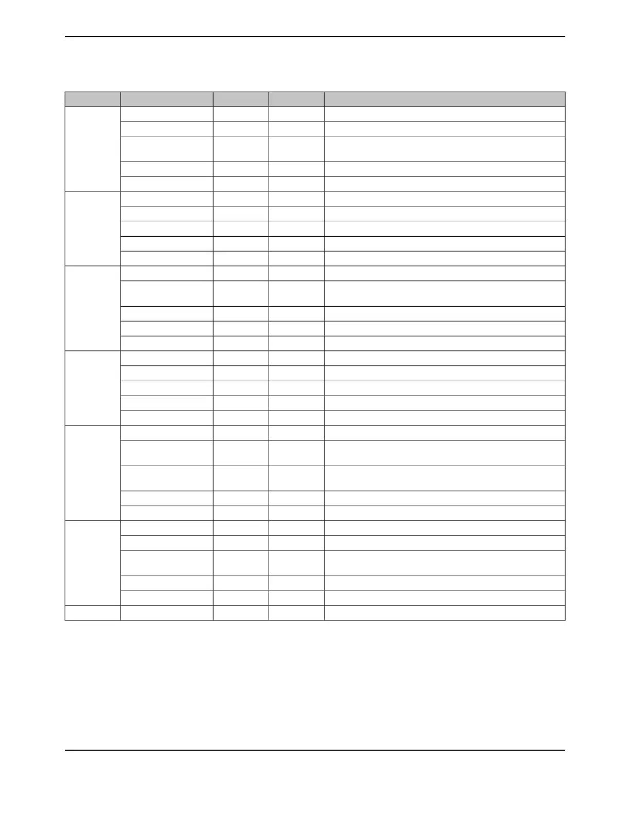
Table 26-2. Signals by Pin Number (continued)
DescriptionBuffer TypePin TypePin NamePin Number
GPIO port A bit 0.TTLI/OPA0
33
CAN module 0 receive.TTLICAN0Rx
I
2
C module 9 clock. Note that this signal has an active pull-up. The
corresponding port pin should not be configured as open drain.
ODI/OI2C9SCL
16/32-Bit Timer 0 Capture/Compare/PWM 0.TTLI/OT0CCP0
UART module 0 receive.TTLIU0Rx
GPIO port A bit 1.TTLI/OPA1
34
CAN module 0 transmit.TTLOCAN0Tx
I
2
C module 9 data.ODI/OI2C9SDA
16/32-Bit Timer 0 Capture/Compare/PWM 1.TTLI/OT0CCP1
UART module 0 transmit.TTLOU0Tx
GPIO port A bit 2.TTLI/OPA2
35
I
2
C module 8 clock. Note that this signal has an active pull-up. The
corresponding port pin should not be configured as open drain.
ODI/OI2C8SCL
SSI module 0 clockTTLI/OSSI0Clk
16/32-Bit Timer 1 Capture/Compare/PWM 0.TTLI/OT1CCP0
UART module 4 receive.TTLIU4Rx
GPIO port A bit 3.TTLI/OPA3
36
I
2
C module 8 data.ODI/OI2C8SDA
SSI module 0 frame signalTTLI/OSSI0Fss
16/32-Bit Timer 1 Capture/Compare/PWM 1.TTLI/OT1CCP1
UART module 4 transmit.TTLOU4Tx
GPIO port A bit 4.TTLI/OPA4
37
I
2
C module 7 clock. Note that this signal has an active pull-up. The
corresponding port pin should not be configured as open drain.
ODI/OI2C7SCL
SSI Module 0 Bi-directional Data Pin 0 (SSI0TX in Legacy SSI
Mode).
TTLI/OSSI0XDAT0
16/32-Bit Timer 2 Capture/Compare/PWM 0.TTLI/OT2CCP0
UART module 3 receive.TTLIU3Rx
GPIO port A bit 5.TTLI/OPA5
38
I
2
C module 7 data.ODI/OI2C7SDA
SSI Module 0 Bi-directional Data Pin 1 (SSI0RX in Legacy SSI
Mode).
TTLI/OSSI0XDAT1
16/32-Bit Timer 2 Capture/Compare/PWM 1.TTLI/OT2CCP1
UART module 3 transmit.TTLOU3Tx
Positive supply for I/O and some logic.Power-VDD
39
June 18, 20141776
Texas Instruments-Production Data
Signal Tables
 Loading...


