IO Wrap Register Map
www.ti.com
1202
SBAU337–May 2020
Submit Documentation Feedback
Copyright © 2020, Texas Instruments Incorporated
Serial Interface Register Maps
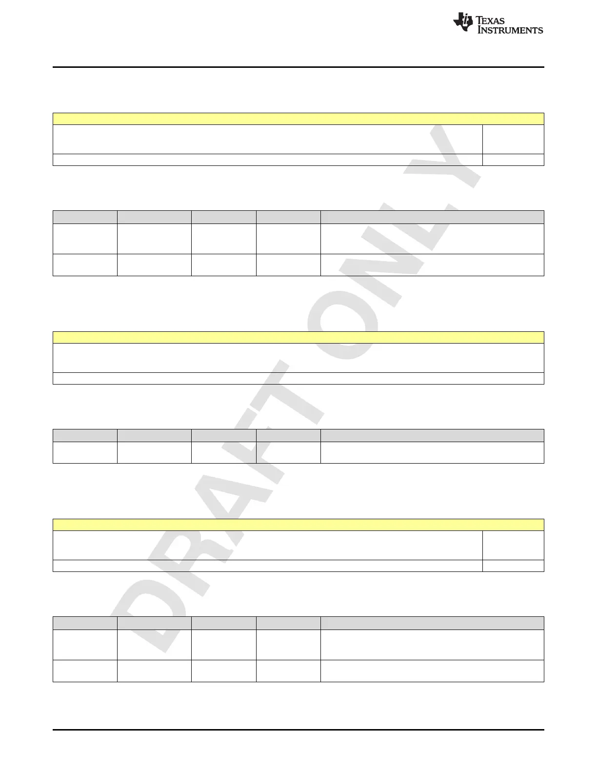
2.16.613 Register 10F1h (offset = 10F1h) [reset = 2h]
Figure 2-2876. Register 10F1h
7 6 5 4 3 2 1 0
OVR_SEL_INT
PO_DAC_SYN
C_N_CD_0
OVR_INTPO_D
AC_SYNC_N_
CD_0
R/W-1h R/W-0h
LEGEND: R/W = Read/Write; W = Write only; -n = value after reset
Table 2-2892. Register 10F1 Field Descriptions
Bit Field Type Reset Description
1-1
OVR_SEL_INTPO_
DAC_SYNC_N_CD
_0
R/W 1h
control to select whether the input function
intpo_dac_sync_n_cd_0 needs to be overriden ot not. 1
indicates override.
0-0
OVR_INTPO_DAC
_SYNC_N_CD_0
R/W 0h
override value for intpo_dac_sync_n_cd_0 when
ovr_sel_intpo_dac_sync_n_cd_0 is made high
2.16.614 Register 10F4h (offset = 10F4h) [reset = 0h]
Figure 2-2877. Register 10F4h
7 6 5 4 3 2 1 0
POL_INTPO_D
AC_SYNC_N_
CD_1
R/W-0h
LEGEND: R/W = Read/Write; W = Write only; -n = value after reset
Table 2-2893. Register 10F4 Field Descriptions
Bit Field Type Reset Description
0-0
POL_INTPO_DAC
_SYNC_N_CD_1
R/W 0h
polarity control for intpo_dac_sync_n_cd_1. 0 indicates pass
through from GPIO when selected 1 indicates inverted signal
2.16.615 Register 10F5h (offset = 10F5h) [reset = 2h]
Figure 2-2878. Register 10F5h
7 6 5 4 3 2 1 0
OVR_SEL_INT
PO_DAC_SYN
C_N_CD_1
OVR_INTPO_D
AC_SYNC_N_
CD_1
R/W-1h R/W-0h
LEGEND: R/W = Read/Write; W = Write only; -n = value after reset
Table 2-2894. Register 10F5 Field Descriptions
Bit Field Type Reset Description
1-1
OVR_SEL_INTPO_
DAC_SYNC_N_CD
_1
R/W 1h
control to select whether the input function
intpo_dac_sync_n_cd_1 needs to be overriden ot not. 1
indicates override.
0-0
OVR_INTPO_DAC
_SYNC_N_CD_1
R/W 0h
override value for intpo_dac_sync_n_cd_1 when
ovr_sel_intpo_dac_sync_n_cd_1 is made high

 Loading...