PLL Register Map
www.ti.com
154
SBAU337–May 2020
Submit Documentation Feedback
Copyright © 2020, Texas Instruments Incorporated
Serial Interface Register Maps
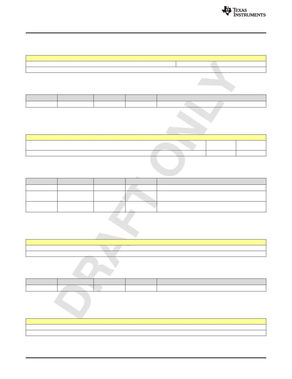
2.2.9 Register 68h (offset = 68h) [reset = 0h]
Figure 2-32. Register 68h
7 6 5 4 3 2 1 0
VCO_SEL_RO
R-0h
LEGEND: R/W = Read/Write; W = Write only; -n = value after reset
Table 2-34. Register 68 Field Descriptions
Bit Field Type Reset Description
2-0 VCO_SEL_RO R 0h VCO bank selection
2.2.10 Register 6Ah (offset = 6Ah) [reset = 0h]
Figure 2-33. Register 6Ah
7 6 5 4 3 2 1 0
reserved LCMGEN_SYN
C_ENA
RST_LOCK_D
ETECT
R/W-0h R/W-0h R/W-0h
LEGEND: R/W = Read/Write; W = Write only; -n = value after reset
Table 2-35. Register 6A Field Descriptions
Bit Field Type Reset Description
7-2 reserved R/W 0h
1-1
LCMGEN_SYNC_
ENA
R/W 0h bit to enable lcm_counter syncing on sysref entering plldig
0-0
RST_LOCK_DETE
CT
R/W 0h Reset PLL lock detection
2.2.11 Register 6Ch (offset = 6Ch) [reset = 0h]
Figure 2-34. Register 6Ch
7 6 5 4 3 2 1 0
LCMGEN_DIV[7:0]
R/W-0h
LEGEND: R/W = Read/Write; W = Write only; -n = value after reset
Table 2-36. Register 6C Field Descriptions
Bit Field Type Reset Description
7-0 LCMGEN_DIV[7:0] R/W 0h lcm counter period (no of lcm clks): set actual N-1 here
2.2.12 Register 6Dh (offset = 6Dh) [reset = 0h]
Figure 2-35. Register 6Dh
7 6 5 4 3 2 1 0
LCMGEN_DIV[15:8]
R/W-0h
LEGEND: R/W = Read/Write; W = Write only; -n = value after reset