FB Top Register Map
www.ti.com
956
SBAU337–May 2020
Submit Documentation Feedback
Copyright © 2020, Texas Instruments Incorporated
Serial Interface Register Maps
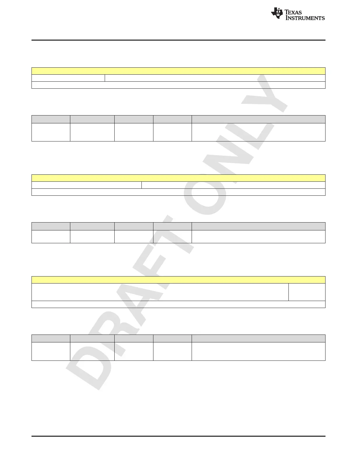
2.14.316 Register 650h (offset = 650h) [reset = 0h]
Figure 2-2199. Register 650h
7 6 5 4 3 2 1 0
FB_ALC_BAND0_EXT_COMP_MIN_ATTN
R/W-0h
LEGEND: R/W = Read/Write; W = Write only; -n = value after reset
Table 2-2213. Register 650 Field Descriptions
Bit Field Type Reset Description
5-0
FB_ALC_BAND0_
EXT_COMP_MIN_
ATTN
R/W 0h
Min value of external DVGA/LNA gain for Band0. DGC will
compensate for gain changes only above this value
2.14.317 Register 712h (offset = 712h) [reset = 0h]
Figure 2-2200. Register 712h
7 6 5 4 3 2 1 0
FB_DDC_PROG_DELAY
R/W-0h
LEGEND: R/W = Read/Write; W = Write only; -n = value after reset
Table 2-2214. Register 712 Field Descriptions
Bit Field Type Reset Description
4-0
FB_DDC_PROG_D
ELAY
R/W 0h
Programmable delay in ADC clock cycles. Valid range 0
through 31
2.14.318 Register 713h (offset = 713h) [reset = 0h]
Figure 2-2201. Register 713h
7 6 5 4 3 2 1 0
FB_DDC_PRO
G_DELAY_BY
PASS
R/W-0h
LEGEND: R/W = Read/Write; W = Write only; -n = value after reset
Table 2-2215. Register 713 Field Descriptions
Bit Field Type Reset Description
0-0
FB_DDC_PROG_D
ELAY_BYPASS
R/W 0h
Bypass the programmable delay block.
1 : Bypass Enable in FB Mode
0 : Bypass Disable in FB Mode

 Loading...

