AFE79xx_GLOBAL Register Map
www.ti.com
146
SBAU337–May 2020
Submit Documentation Feedback
Copyright © 2020, Texas Instruments Incorporated
Serial Interface Register Maps
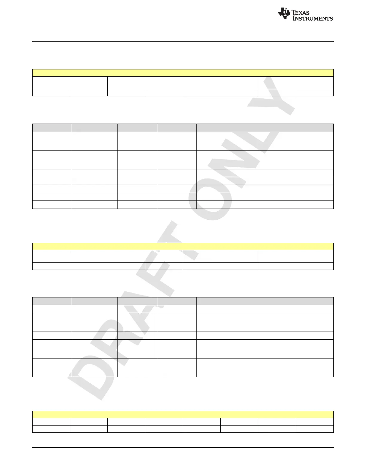
2.1.15 Register 15h (offset = 15h) [reset = 0h]
Figure 2-15. Register 15h
7 6 5 4 3 2 1 0
TIMING_CONT
ROLLER
DIGTOP reserved IO_WRAP reserved ANA_4T4R PLL
R/W-0h R/W-0h R/W-0h R/W-0h R/W-0h R/W-0h R/W-0h
LEGEND: R/W = Read/Write; W = Write only; -n = value after reset
Table 2-16. Register 15 Field Descriptions
Bit Field Type Reset Description
7-7
TIMING_CONTRO
LLER
R/W 0h
page enable for timing controller.
0 : disable
1 : enable
6-6 DIGTOP R/W 0h
page enable for Misc Digital Control
0 : disable
1 : enable
5-5 reserved R/W 0h
4-4 IO_WRAP R/W 0h Page select for GPIO control registers
3-2 reserved R/W 0h 0
1-1 ANA_4T4R R/W 0h Page select for analog 4t4r page.
0-0 PLL R/W 0h Page select for PLL control registers
2.1.16 Register 16h (offset = 16h) [reset = 0h]
Figure 2-16. Register 16h
7 6 5 4 3 2 1 0
0 SERDES JESD_SUBCHI
P
DAC_JESD ADC_JESD
R/W-0h R/W-0h R/W-0h R/W-0h R/W-0h
LEGEND: R/W = Read/Write; W = Write only; -n = value after reset
Table 2-17. Register 16 Field Descriptions
Bit Field Type Reset Description
7-7 0 R/W 0h Must read or write 0
6-5 SERDES R/W 0h
Page select for Serdes PHY registers
Bit0 --> for serdes_0
Bit1 --> for serdes_1
4-4 JESD_SUBCHIP R/W 0h Page select for JESD SUBCHIP registers.
3-2 DAC_JESD R/W 0h
Page select for DAC JESD control registers
Bit0 --> for DAC_JESD_AB
Bit1 --> for DAC_JESD_CD
1-0 ADC_JESD R/W 0h
Page select for ADC_Jesd control registers
Bit0 --> ADC_JESD_AB
Bit1 --> ADC_JESD_CD
2.1.17 Register 18h (offset = 18h) [reset = 0h]
Figure 2-17. Register 18h
7 6 5 4 3 2 1 0
calib_memory reserved MACRO reserved MCU_mem reserved reserved reserved
R/W-0h R/W-0h R/W-0h R/W-0h R/W-0h R/W-0h R/W-0h R/W-0h
LEGEND: R/W = Read/Write; W = Write only; -n = value after reset

 Loading...

