www.ti.com
SERDES Register Map
467
SBAU337–May 2020
Submit Documentation Feedback
Copyright © 2020, Texas Instruments Incorporated
Serial Interface Register Maps
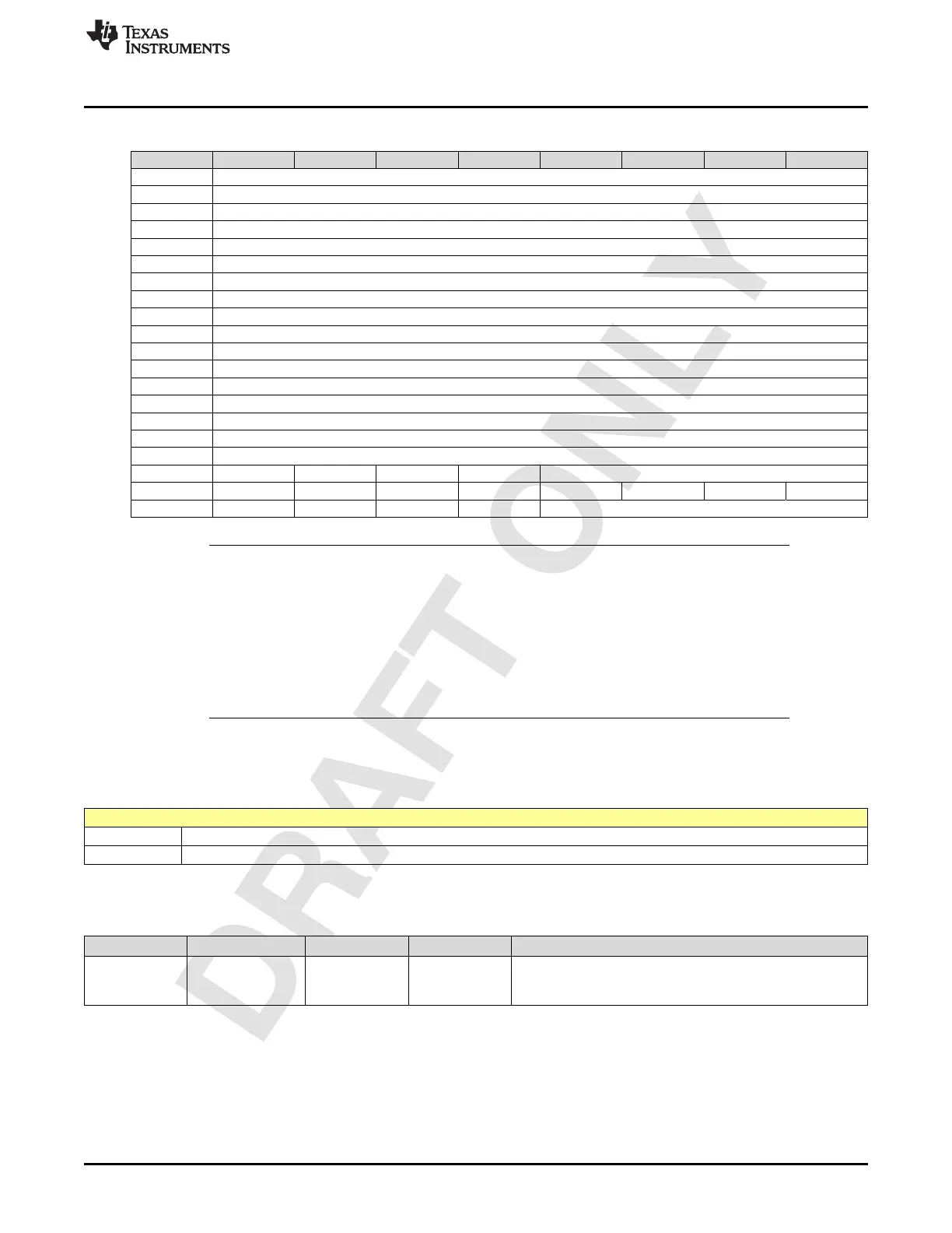
Table 2-720. Serdes Register Map (continued)
ADDRESS (Hex) D7 D6 D5 D4 D3 D2 D1 D0
7E0Dh FIRMWARE_DATA6[15:8]
7E0Eh FIRMWARE_DATA7[7:0]
7E0Fh FIRMWARE_DATA7[15:8]
7E10h FIRMWARE_DATA8[7:0]
7E11h FIRMWARE_DATA8[15:8]
7E12h FIRMWARE_DATA9[7:0]
7E13h FIRMWARE_DATA9[15:8]
7E14h FIRMWARE_DATAA[7:0]
7E15h FIRMWARE_DATAA[15:8]
7E16h FIRMWARE_DATAB[7:0]
7E17h FIRMWARE_DATAB[15:8]
7E18h RAM_ADDRESS_HIGH[7:0]
7E19h RAM_ADDRESS_HIGH[15:8]
7E1Ah RAM_ADDRESS_LOW[7:0]
7E1Bh RAM_ADDRESS_LOW[15:8]
7E1Ch FIRMWARE_CHECKSUM[7:0]
7E1Dh FIRMWARE_CHECKSUM[15:8]
7E1Eh FRAME_LEN
7E1Fh MCU_WRITE MCU_START CHKSUM_ERR
7E20h DUMMYPAGESELECT
NOTE: The registers with address 0x40zz and 0x41zz are per lane registers and they can be
extended to other lanes using the following map values instead of 0x40zz and 0x41zz. For
serdes_0 lanes - SRX1/STX1 – 0x42zz and 0x43zz, SRX2/STX2 – 0x40zz and 0x41zz,
SRX3/STX3 – 0x44zz and 0x45zz, SRX4/STX4 – 0x46zz and 0x47zz.
For serdes_1 lanes – SRX5/STX5 – 0x46zz and 0x47zz, SRX6/STX6 – 0x44zz and 0x45zz,
SRX7/STX7 – 0x40zz and 0x41zz, SRX8/STX8 – 0x42zz and 0x43zz.
The registers with addresses – 0x48zz,0x49zz,0x6Ezz,0x70zz and 0x7Ezz are the common
registers per 4 lanes.
2.6.1 Register 4000h (offset = 4000h) [reset = 0h]
Figure 2-715. Register 4000h
7 6 5 4 3 2 1 0
DFE_MODE
R/W-0h
LEGEND: R/W = Read/Write; W = Write only; -n = value after reset
Table 2-721. Register 4000 Field Descriptions
Bit Field Type Reset Description
7-7 DFE_MODE R/W 0h
RX DFE Mode selector
0h: 1 Tap DFE
1h: Disable DFE

 Loading...

