SERDES Register Map
www.ti.com
504
SBAU337–May 2020
Submit Documentation Feedback
Copyright © 2020, Texas Instruments Incorporated
Serial Interface Register Maps
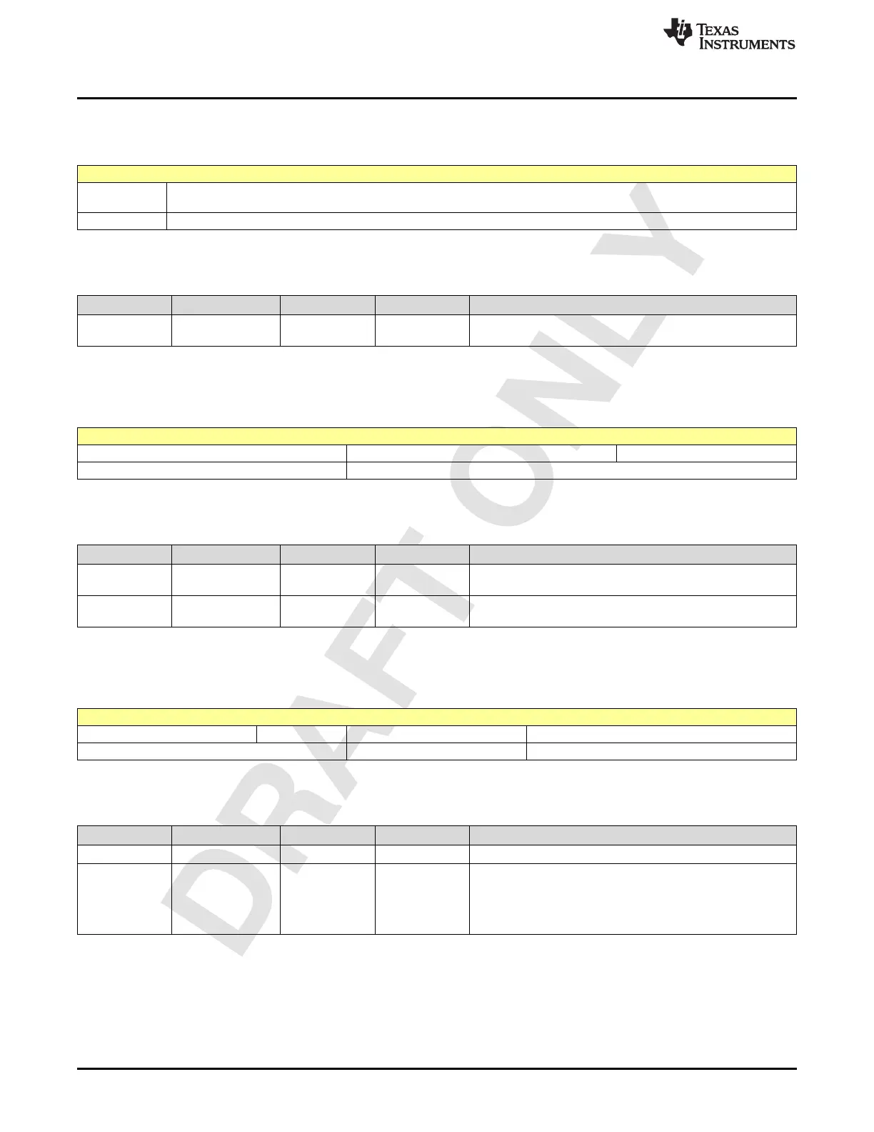
2.6.121 Register 49DCh (offset = 49DCh) [reset = 0h]
Figure 2-835. Register 49DCh
7 6 5 4 3 2 1 0
RX_SLICER_BI
AS_LANE0[0]
R/W-0h
LEGEND: R/W = Read/Write; W = Write only; -n = value after reset
Table 2-841. Register 49DC Field Descriptions
Bit Field Type Reset Description
7-7
RX_SLICER_BIAS
_LANE0[0]
R/W 0h Controls the RX slicer bias setting for lane 1.
2.6.122 Register 49DDh (offset = 49DDh) [reset = 60h]
Figure 2-836. Register 49DDh
7 6 5 4 3 2 1 0
RX_AGCBUFDAC_LANE0 RX_SLICER_BIAS_LANE0[2:1]
R/W-3h R/W-0h
LEGEND: R/W = Read/Write; W = Write only; -n = value after reset
Table 2-842. Register 49DD Field Descriptions
Bit Field Type Reset Description
7-5
RX_AGCBUFDAC_
LANE0
R/W 3h Controls AGC output driver for lane 1.
1-0
RX_SLICER_BIAS
_LANE0[2:1]
R/W 0h Controls the RX slicer bias setting for lane 1.
2.6.123 Register 49DEh (offset = 49DEh) [reset = 0h]
Figure 2-837. Register 49DEh
7 6 5 4 3 2 1 0
TX_INTP_DIS REFCLK_DIV
R/W-0h R/W-0h
LEGEND: R/W = Read/Write; W = Write only; -n = value after reset
Table 2-843. Register 49DE Field Descriptions
Bit Field Type Reset Description
5-5 TX_INTP_DIS R/W 0h Disables TX interpolator when set to 1.
4-3 REFCLK_DIV R/W 0h
Mux control bit that controls the recovered clock divide.
00h: /320 (Default)
01h: /160 (Required)
10h: Invalid. Do not use.
11h: Invalid. Do not use.