ADSP-214xx SHARC Processor Hardware Reference A-177
Registers Reference
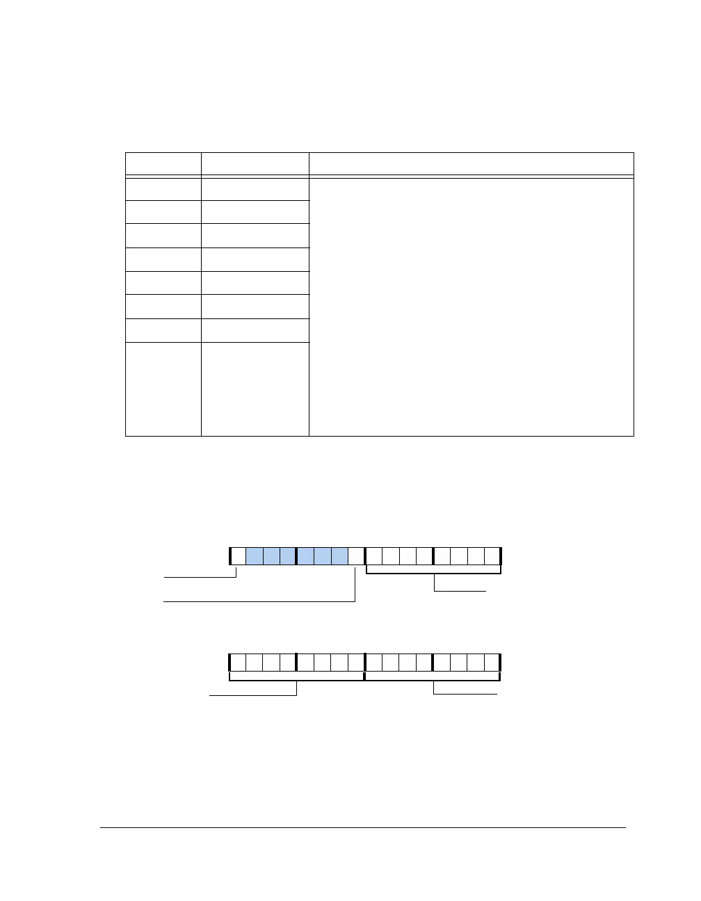
Input Data Port Control Register 1 (IDP_CTL1)
Use the
IDP_CTL1 register to configure and enable individual IDP chan-
nels. The register is shown in Figure A-94 and described in Table A-91.
10–8 IDP_SMODE0 Serial Input Data Format Mode Select. These eight inputs (0–
7), each of which contains 3 bits, indicate the mode of the
serial input for each of the eight IDP channels.
Input format:
000 = Left-justified 24 bits
001 = I
2
S mode 24 bits
010 = Left-justified 32 bits
011 = I
2
S 32 bits
100 = Right-justified 24 bits
101 = Right-justified 20 bits
110 = Right-justified 18 bits
111 = Right-justified 16 bits
Note the SMODEx bits define the IDP buffer input format
for core access. For I2S and left-justified single channel modes,
it receives 32 bits of data from the SDATA pins. No L/R bit is
added in these modes.
13–11 IDP_SMODE1
16–14 IDP_SMODE2
19–17 IDP_SMODE3
22–20 IDP_SMODE4
25–23 IDP_SMODE5
28–26 IDP_SMODE6
31–29 IDP_SMODE7
Figure A-94. IDP_CTL1 Register
Table A-90. IDP_CTL0 Register Bit Descriptions (RW) (Cont’d)
Bits Name Description
IDP_ENx (7–0)
IDP Channel x Enable
IDP_DMA_ENx (15–8)
IDP Channel x DMA Enable
IDP_PINGx (23–16)
IDP Channel x Ping-pong
DMA Enable
IDP_FFCLR
Clear IDP FIFO
IDP_INTEN
Independent Channel
Synchronization Enable
31 302928 27 26 25 24 23 22 21 20 19 18 17 16
09 837564 2114 12 11 101315

 Loading...

