ADSP-2146x External Port Registers
A-40 ADSP-214xx SHARC Processor Hardware Reference
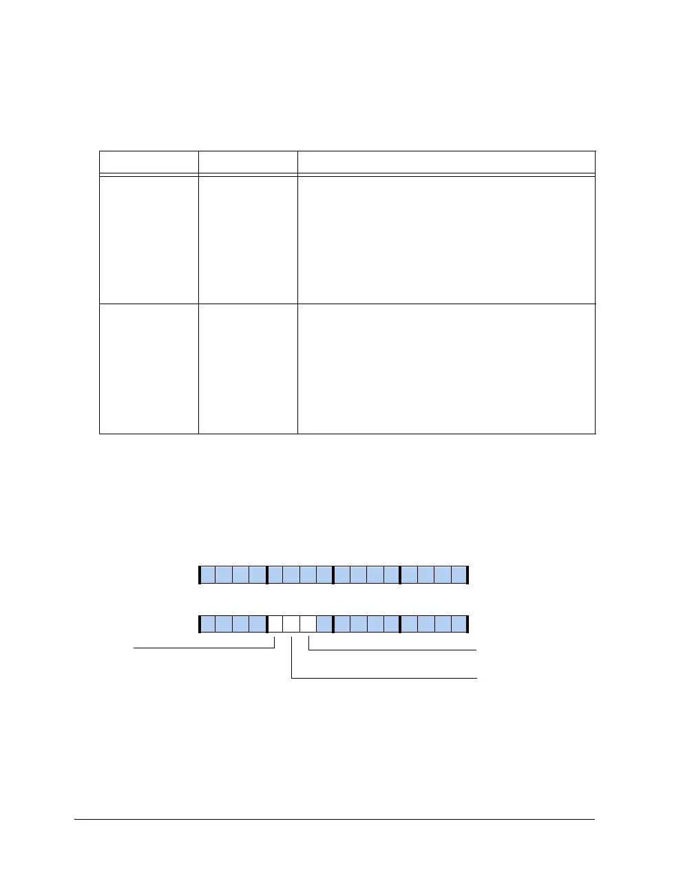
DLL0 Control Register 1 (DLL0CTL1)
The
DLL0CTL1 register shown in Figure A-16 and described in Table A-20
includes the programmable parameters associated with the DLL0 device.
Note that it takes at least 9 core clock cycles to perform a DLL reset.
23–16 External Bank 2
Status
External Bank 0 Active/Precharge State.
xxxxxxx1 = Internal bank 0 in open state
xxxxxxx0 = Internal bank 0 in precharge state
xxxxxx1x = Internal bank 1 in open state
xxxxxx0x = Internal bank 1 in precharge state
…
1xxxxxxx = Internal bank 7 in open state
0xxxxxxx = Internal bank 7 in precharge state
31–24 External Bank 3
Status
External Bank 0 Active/Precharge State.
xxxxxxx1 = Internal bank 0 in open state
xxxxxxx0 = Internal bank 0 in precharge state
xxxxxx1x = Internal bank 1 in open state
xxxxxx0x = Internal bank 1 in precharge state
…
1xxxxxxx = Internal bank 7 in open state
0xxxxxxx = Internal bank 7 in precharge state
Figure A-16. DLL0CTL1 Register
Table A-19. DDR2STAT1 Register Bit Descriptions (RO) (Cont’d)
Bit Field Field Name Description
RESETDLL
RESETDAT
Reset Data Capture Logic
Reset DLL Control Logic
31 302928 27 26 25 24 23 22 21 20 19 18 17 16
09 837564 2114 12 11 101315
RESETCAL
Reset the DQS Phase Cali-
bration Logic

 Loading...

