ADSP-214xx SHARC Processor Hardware Reference 22-5
Power Management
PLL VCO
The VCO is the PLL output stage of the PLL. It feeds the output clock
generator which provides core and peripheral clocks as shown in
Table 22-1. Two settings have an impact on the VCO frequency:
• The
INDIV bit enables the CLKIN input pre-divider by 2.
• The
PLLM bits and the CLK_CFG1–0 pins control the PLL multiplier
unit.
Changing the VCO frequency requires a new condition for the PLL cir-
cuitry. Therefore, the core needs to wait a specific settling time in bypass
mode before it can be released for further activities (typically 4096 CLKIN
cycles).
Output Clock Generator
The output clock generator post divides the VCO clock to the core ratio
or peripherals ratio and synchronizes all output clocks. It is fed with the
VCO clock and does not provide any feedback back to the PLL circuit.
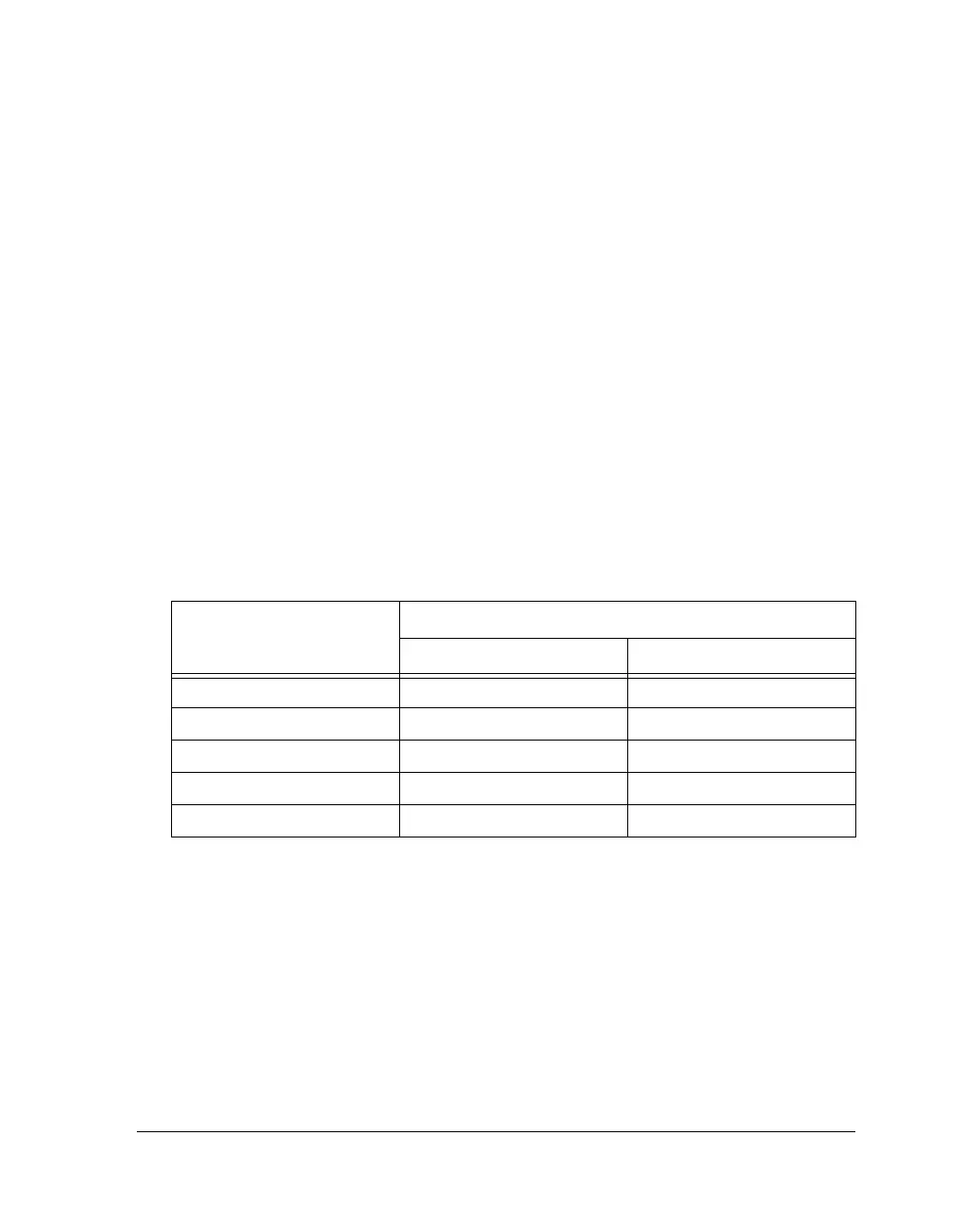
Table 22-1. VCO Encodings
PLLM Bit Settings
VCO Frequency
1
1 For operational limits for the VCO clock see the appropriate product data sheet.
INDIV = 0 INDIV = 1
0 128x 64x
12x1x
24x2x
N = 3–62 2Nx Nx
63 126x 63x

 Loading...

