ADSP-214xx SHARC Processor Hardware Reference 22-7
Power Management
phase-locked loop. Note that the goal in selecting a particular clock ratio
for an application is to provide the highest permissible internal frequency
for a given
CLKIN frequency. For more information on available clock
rates, see the appropriate product data sheet.
Operating Modes
The following sections provide information on the various options for
clock operation.
Bypass Mode
Bypass mode must be used if any runtime VCO clock change is required.
Setting the PLLBP bit bypasses the entire PLL circuitry. In bypass mode,
the core runs at
CLKIN speed. Once the PLL has settled into the new VCO
frequency, (which may take 4096
CLKIN cycles) the PLLBP bit may be
cleared to release the core from bypass mode. For more information, see
“Back to Back Bypass” on page 22-17.
Only VCO frequency changes require bypass mode, therefore this
mode is not intended as a standard operating mode.
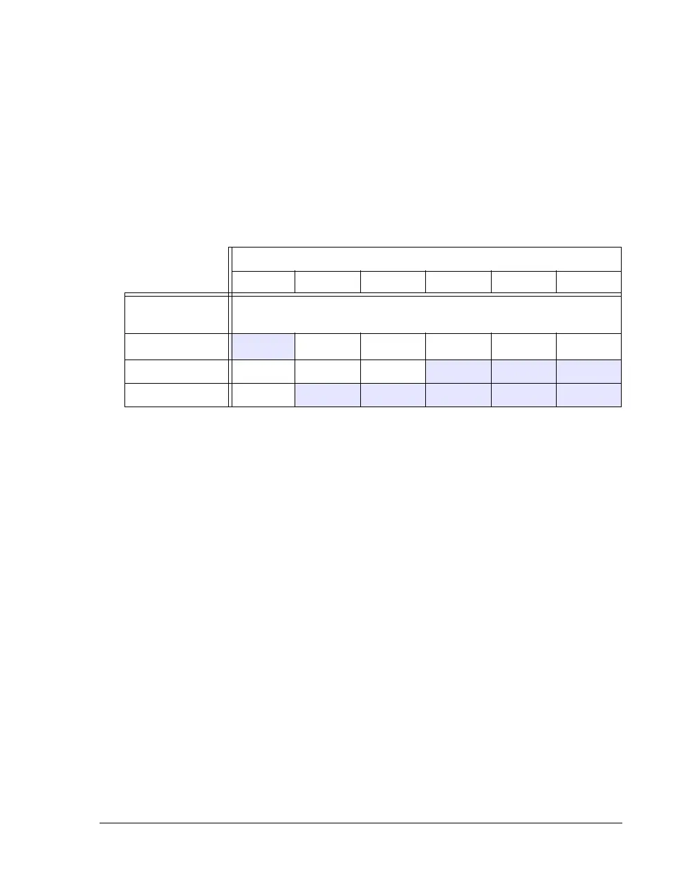
Table 22-2. Selecting Core to CLKIN Ratio (ADSP-2146x)
Typical Crystal and Clock Oscillators Inputs
12.500 16.667 25.000 33.333 40.000 50.000
Clock Ratios
(CLK_CFG Pins)
Core CLK (MHz)
1
1 For operational limits for the core clock frequency see the appropriate product data sheet.
6:1
2
2 For ADSP-2147x and ADSP-2148x models, the ratio is 8:1.
N/A 100 150 200 240 300
16:1 200 266.66 400 N/A N/A N/A
32:1 400
N/A N/A N/A N/A N/A

 Loading...

