ADSP-214xx SHARC Processor Hardware Reference 17-3
Shift Register – ADSP-2147x
Pin Descriptions
The pin descriptions for the shift register are described in the
ADSP-2147x data sheet.
SRU Programming
To use the shift register, route the required inputs using the SRU as
described in Table 17-2, taking not of the following.
• The SR_SCLK, SR_LAT, and SR_SDI inputs must come from the same
source except in the case where SR_SCLK comes from PCGA/B or
SR_SCLK and SR_LAT come from PCGA/B. If SR_SCLK comes from
PCGA/B then SPORT0–7 generates the SR_LAT and SR_SDI signals. If
SR_SCLK and SR_LAT come from PCGA/B, then SPORT0–7 generates
the SR_SDI signal.
• Configure CKRE = 1 when using SPORT as a source of SR_SCLK_I,
SR_LAT_I, and SR_DAT_I signals.
• The SR_CTL, SRU_CLK_SHREG, and SRU_DAT_SHREG registers are in
PCLK domain. There may be timing violations for signals crossing
PCLK domain to the SR_SDCLK_I and SR_LAT_I domain. To avoid
this first program
SR_CTL, SRU_CLK_SHREG, and SRU_DAT_SHREG reg-
isters and then drive on
SR_SDCLK_I, SR_LAT_I, and SR_SDI_I.
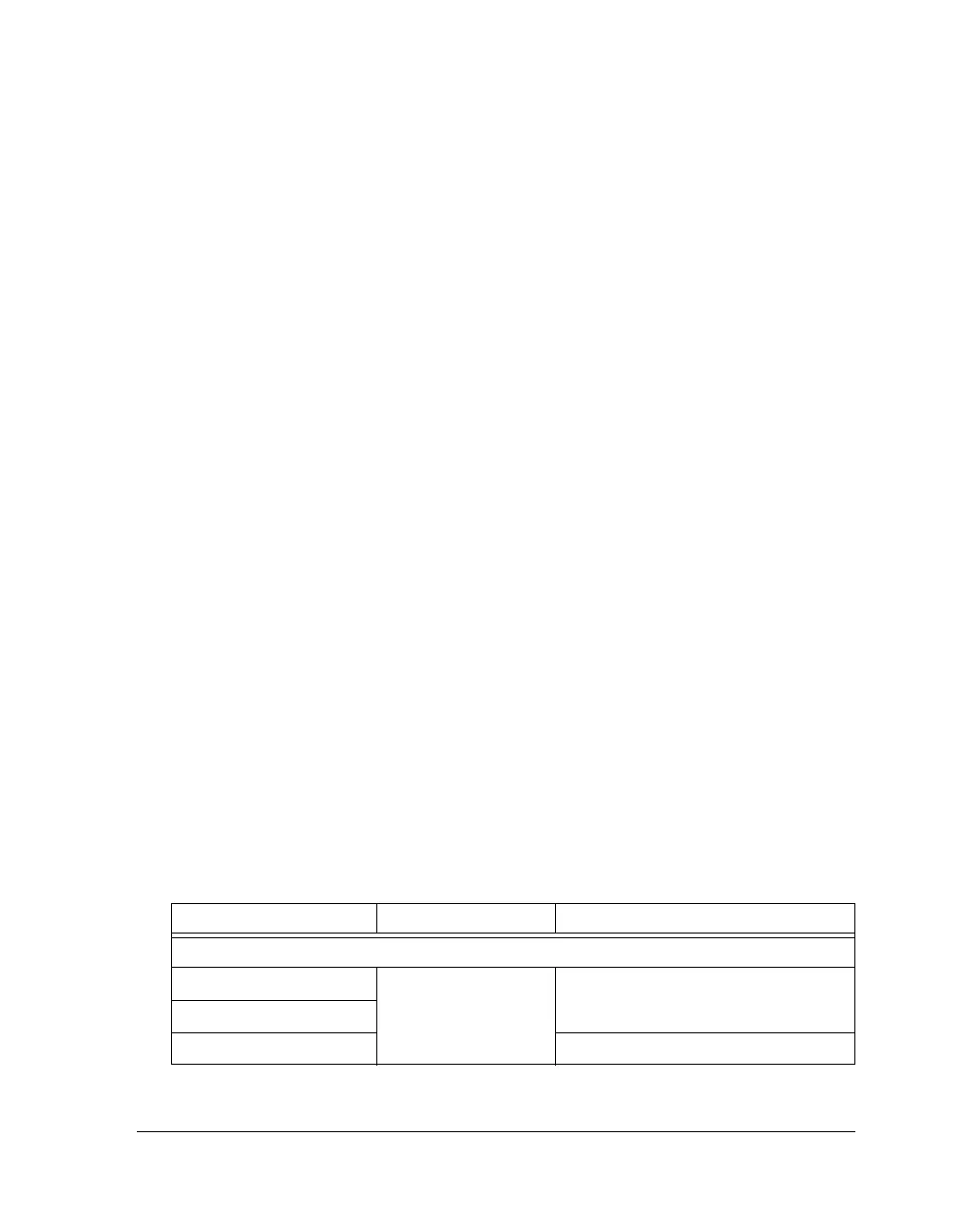
Table 17-2. SR DAI/SRU Connections
Internal Nodes DAI Group SRU Register
Inputs
SR_SCLK_I G SRU_CLK_SHREG
SR_LAT_I
SR_DAT_I SRU_DAT_SHREG

 Loading...

