ADSP-214xx SHARC Processor Hardware Reference 17-7
Shift Register – ADSP-2147x
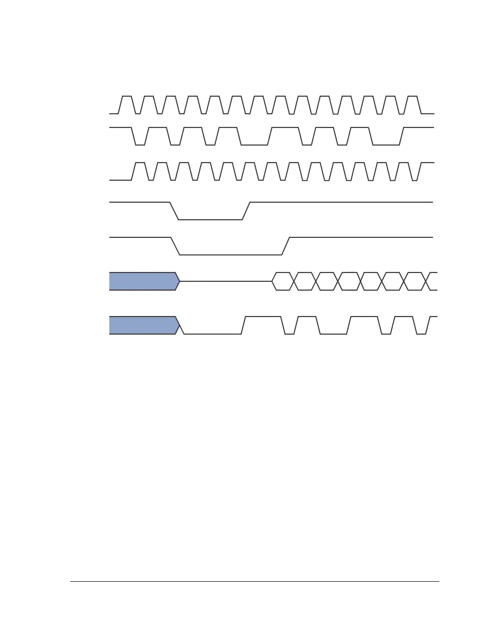
Parallel Data Output
If the SR_LDOE bit in the SR_CTL register is set, the output stage of the par-
allel data latch is enabled. Data in the latch appears at the output
whenever this bit is set.
The data in each flip-flop is transferred to the respective latch on a posi-
tive-going transition of the SR_LAT_I input. If both clocks are connected
together, the shift register is always one clock pulse ahead of the latch.
Figure 17-2. Shift Register Timing
0x00035
SR_SDCLK
0x00003 0x000D60x0006A0x0001A0x0000D0x00006
SR_SDI
SR_LAT
RESET/
SR_CTL1/
SR_CLR
SR_LDOE
SR_LDO
SR_SDO
(LSB)

 Loading...

