DDR2 DRAM Controller (ADSP-2146x)
3-56 ADSP-214xx SHARC Processor Hardware Reference
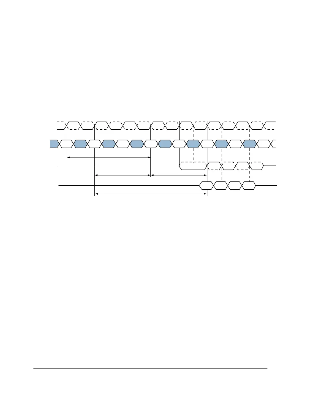
The subsequent burst bit data are issued on successive edges of
DDR2_DQS
until the burst length is completed. When the burst has finished, any
additional data supplied to the DDR2_DATA pins is ignored. The DDR2_DATA
signal is ignored after the burst write operation is complete. The time
from the completion of the burst write to bank precharge is the write
recovery time (WR).
Auto-Refresh
The DDR2 internally increments the refresh address counter and causes a
CAS before RAS (CBR) refresh to occur internally for that address when
the auto-refresh command is given. The controller generates an
auto-refresh command after the refresh counter times out. The RDIV value
in the
DDR2RRC register must be set so that all addresses are refreshed
within the t
REF
period specified in the DDR2 timing specifications.
Before executing the auto-refresh command, the DDR controller executes
a pre-charge all command to all external banks. The next activate com-
mand is not given until the t
RFC
specification is met. Auto-refresh
commands are also issued by the controller as part of the power-up
sequence and after exiting self-refresh mode.
Figure 3-13. Burst Write
T0 T1 T4 T5T2 T3 T7T6
CMD
WL = AL + CL
-
1 = 4
DQS
AL = 2
CL
-
1 = 2
t
RCD (min)
DDR2_DQS/
DDR2_DQS
DDR2_CLKx/
DDR2_CLKx
WRITE
N
NOP NOPNOPNOP NOP NOP
ACTIVE
N
CAS Latency (CL) = 3
Additive Latence (AL) = 2
WRITE latency = AL + CL
-
1 = 4
D
in
n+1
D
in
n+2
D
in
n
D
in
n+3

 Loading...

