DPI Signal Routing Unit Registers
A-218 ADSP-214xx SHARC Processor Hardware Reference
DPI Signal Routing Unit Registers
The digital peripheral interface is comprised of a group of peripherals and
the signal routing unit 2 (SRU2).
Miscellaneous Signal Routing Registers
(SRU2_INPUTx, Group A)
Group A is used to route the 14 external pin signals to the inputs of the
other peripherals. The
MISCBx_O outputs route to the interrupt latch bits
or the pin buffer enable signals (PBEN).
All clock inputs that are not used should be set to logic low. The registers
and input signals for group A are summarized in Figure A-118 through
Figure A-123 and Table A-118.
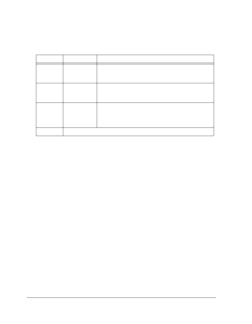
Table A-117. SR_CTL Register Bit Descriptions (RW)
Bit Name Description
0 SR_LDOE Parallel Data Output Enable. This bit enables the parallel
SR_LD017–0 output pins. It is cleared on chip reset (RESET)
and/or asynchronously on external SR_CLR pin.
1 SR_SW_CLR Software Clear/Reset. If this bit is 0, then the reset is active.
0 = Shift register cleared
1 = Shift register enabled
6–2 SR_SDO_SEL Serial Data Out Multiplexer’s Select Input. These bits select
which parallel word is shifted through the SR_SDO pin.
00000 = LSB selected.
10001 = MSB selected.
31–7 Reserved

 Loading...

