Functional Description
9-8 ADSP-214xx SHARC Processor Hardware Reference
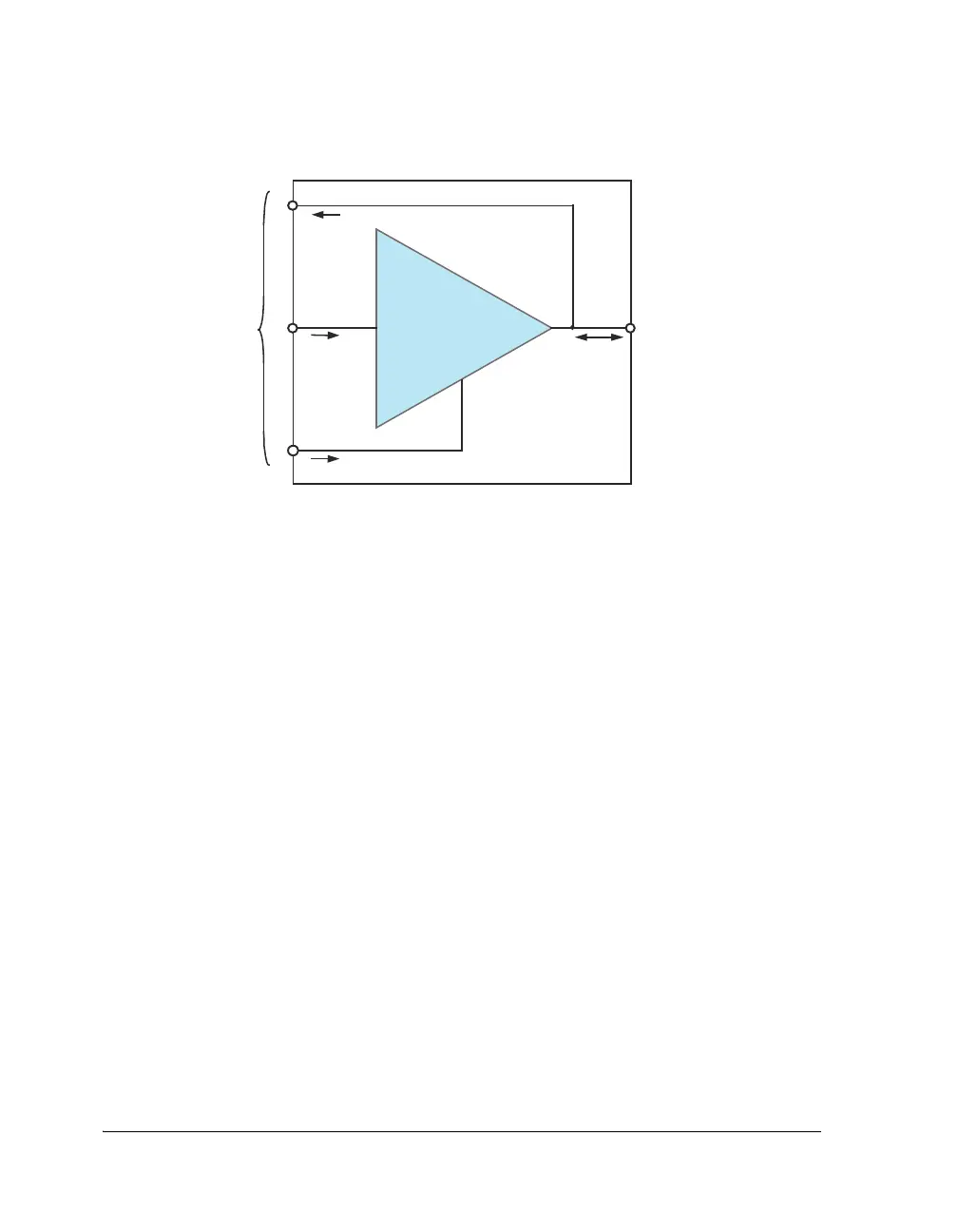
The notation for pin input and output connections can be quite confusing
at first because, in a typical system, a pin is simply a wire that connects to
a device. The manner in which the pins are routed within the SRU
requires additional nomenclature. The pin interface’s input may be
thought of as the input to a buffer amplifier that can drive a load on the
physical external lead. The pin interface enable is the input signal that
enables the output of the buffer by turning it on when its value is logic
high, and turning it off when its value is logic low.
When the pin enable is asserted, the pin output is logically equal to pin
input, and the pin is driven. When the pin enable is deasserted, the output
of the buffer amplifier becomes high impedance. In this situation, an
external device may drive a level onto the line, and the pin is used as an
input to the processors.
Pin Buffers as Signal Output
In a typical embedded system, most pins are designated as either inputs or
outputs when the circuit is designed, even though they may have the abil-
ity to be used in either direction. Each of the DAI pins can be used as
Figure 9-3. Pin Buffer Example
IN
OUT
ENABLE
DAI_PBxx_I
DAI_PBxx_O
PBENxx_I
External DAI
pin buffer
Interface
to SRU
PIN
BUFFER

 Loading...

