Functional Description
14-6 ADSP-214xx SHARC Processor Hardware Reference
Functional Description
The following sections provide information on the function of the preci-
sion clock generators.
Serial Clock
Each of the four units (A, B, C, and D) produces a clock output. Serial
clock generation from a unit is independently enabled and controlled.
Sources for the serial clock generation can be either from the
CLKIN, PCLK,
or a DAI pin source. The clock output is derived from the input to the
PCG with a 20-bit divisor.
Note that the divider is working in normal mode for CLKDIV > 1. For
CLKDIV = 0, 1 the divider operates in bypass mode, (input clock is fed
directly to its output). Note that in bypass mode, the clock at the output
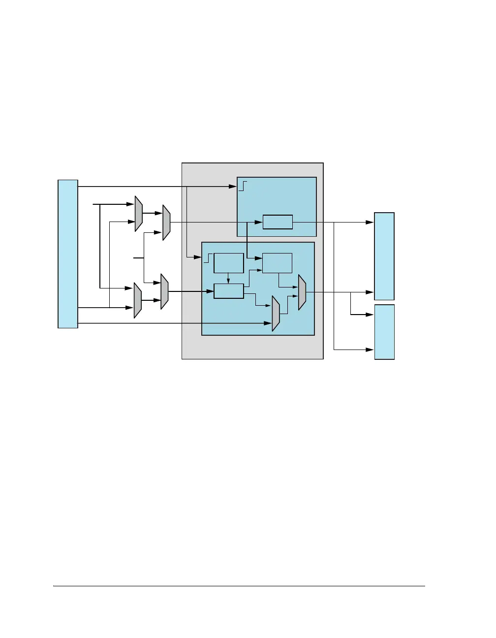
Figure 14-1. PCG Block Diagram
PCG_SYNC_CLKx_I
MISCA5
-
2_I
PCG_
FSCD_O
PCG_CLK
CD_O
PCG_
CLKABCD_O
PCG_EXTx_I
DPI
IN
PCLK
CLKIN
Ext. Event Trigger
CLKDIV
FSDIV
PULSE
WIDTH
One Shot
PCG_
FSABCD_O
PERCISION CLOCK
GENERATOR
FRAME SYNC
FS
PHASE
DAI
IN
Normal (>1)
Bypass (0,1)
SCLK
Normal (>1)
Bypass (0,1)
DAI
OUT

 Loading...

