ADSP-214xx SHARC Processor Hardware Reference 3-55
External Port
Each subsequent data-out appears on the
DDR2_DATA pin in phase with the
DDR2_DQS signal in a source synchronous manner.
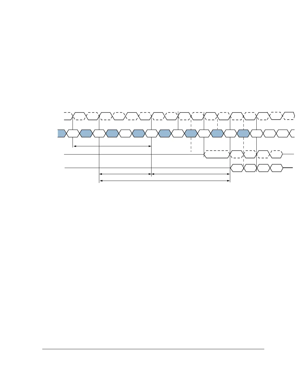
The RL is equal to an additive latency (AL) plus CAS latency (CL). The
CL is defined by the mode register (MR), similar to the existing SDRAM.
The AL is defined by the EMR1 register.
Burst Write
The burst write command, shown in Figure 3-13, is initiated by having
DDR2_CS, DDR2_CAS and DDR2_WE pins low while holding DDR2_RAS high at
the rising edge of the clock. The address inputs determine the starting col-
umn address. Write latency (WL) is defined by a read latency (RL) minus
one and is equal to (AL + CL – 1) and is the number of clocks of delay
that are required from the time the write command is registered to the
clock edge associated to the first
DDR2_DQS strobe.
A data strobe signal (
DDR2_DQS) should be driven low (preamble) nomi-
nally a 1/2 clock prior to the WL. The first data bit of the burst cycle must
be applied to the
DDR2_DATA pins at the first rising edge of DDR2_DQS fol-
lowing the preamble.
Figure 3-12. Burst Read
T0 T1 T4 T5T2 T3 T7T6
CMD
RL
-
5
DQ
AL
-
2
CL
-
3
DDR2_DQS/
DDR2_DQS
DDR2_CLKx/
DDR2_CLKx
READ
N
NOP NOPNOPNOP NOP NOP
ACTIVE
N
CAS Latency (CL) = 3
Additive Latence (AL) = 2
READ latency = RL
-
AL + CL
-
5
t
AC,
t
DQSCK,
t
DQSQ = NOMINAL
D
out
n+1
D
out
n+2
D
out
n
D
out
n+3
T8
t
RCD (MIN)

 Loading...

