ADSP-214xx SHARC Processor Hardware Reference A-33
Registers Reference
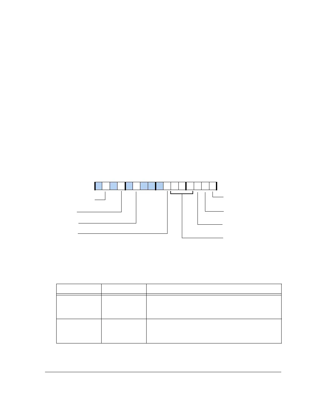
DDR2 Control Register 3 (DDR2CTL3)
The
DDR2CTL3 register includes the programmable parameters associated
with the DDR2 extended mode register (EMR1). Figure A-12 and
Table A-14 show the DDR2 control register 3 bit definitions. All the val-
ues are defined in terms of number of clock cycles. Values written into this
register are loaded into the DDR2 extended mode register during power
up (or when
Force EMR bit in DDR2CTL0 is set). This register should be ini-
tialized before starting the initialization sequence.
This register’s contents should not be changed while DDR2 inter-
face is active. Also, whenever this register’s contents are changed,
an initialization sequence must be executed to reflect this register
contents in to the DDR2 extended mode register.
Figure A-12. DDR2CTL3 Register
Table A-14. DDR2CTL3 Register Bit Descriptions (RW)
Bit Name Description
0 DDR2DLLEN DLL Enable.
0 = DLL enabled
1 = DLL disabled
1 DDR2OPDS Output Drive Strength.
0 = Full strength
1 = Reduced strength
DDR2DLLEN
DDR2OPDS
Output Drive Strength
DLL Enable
DDR2ODT150
On Die Termination
DDR2AL (5–3)
Additive Latency
DDR2DQSDIS
DQS Enable
DDR2EXTMR1 (15–14)
Mode Register 1
DDR2ODT75
On Die Termination
DDR2OBDIS
Output Buffer Disable
09 837564 2114 12 11 101315

 Loading...

