ADSP-214xx SHARC Processor Hardware Reference 11-3
Input Data Port
Pin Descriptions
Table 11-2 provides descriptions of the IDP pins used for the serial inter-
face port.
Table 11-3 provides descriptions of the IDP pins used for the parallel
interface port.
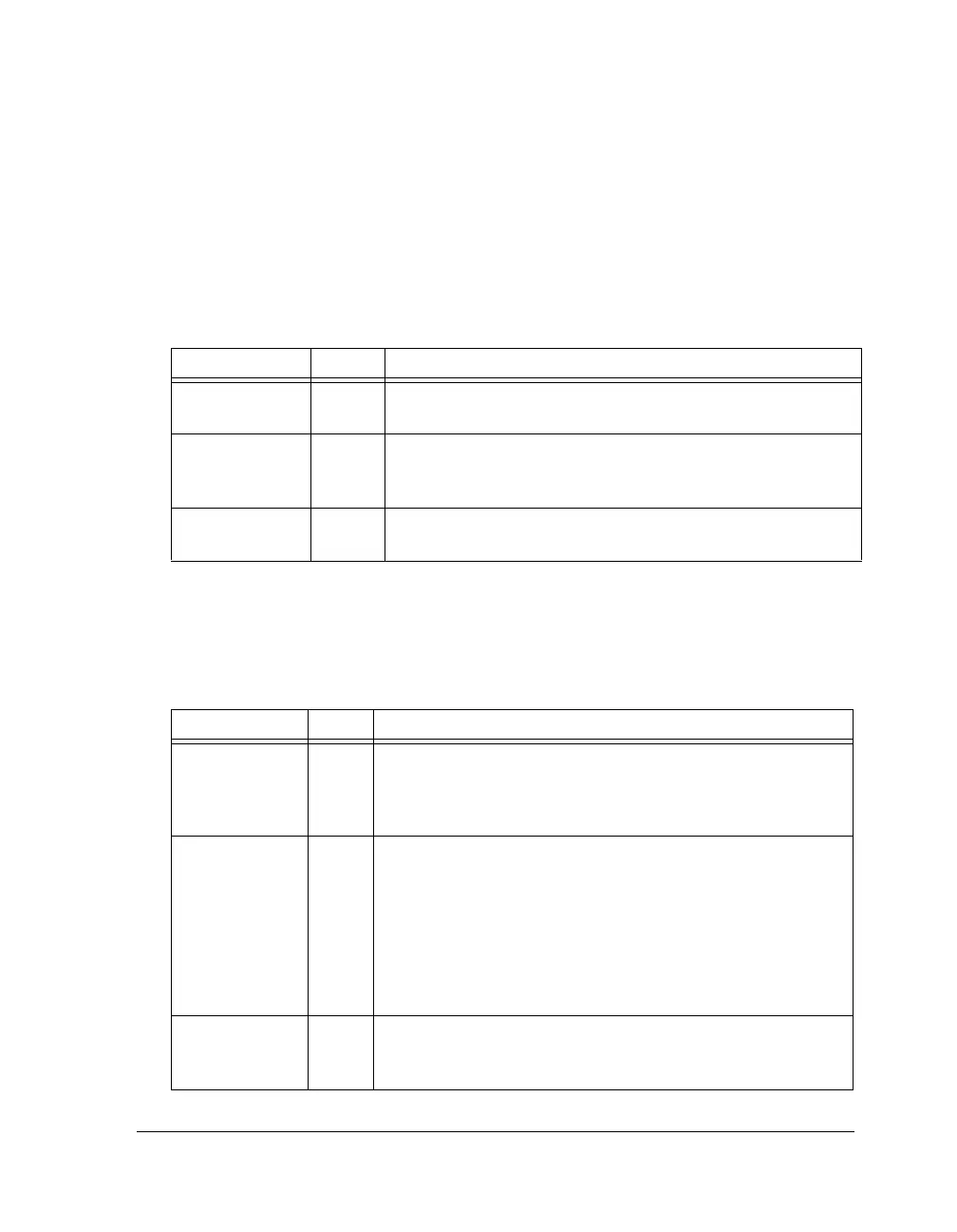
Table 11-2. SIP Pin Descriptions
Internal Node I/O Description
IDP7–0_CLK_I I Serial Input Port Receive Clock Input. This signal must be gener-
ated externally and comply to the supported input formats.
IDP7–0_FS_I I Serial Input Port Frame Sync Input. The frame sync pulse initiates
shifting of serial data. This signal must be generated externally and
comply to the supported input formats.
IDP7–0_DAT_I I Serial Input Port Data Input. Unidirectional data pin. Data signal
must comply to the supported data formats.
Table 11-3. PDAP Pin Descriptions
Internal Nodes Type Description
PDAP_CLK_I I Parallel Data Acquisition Port Clock Input. Positive or negative
edge of the PDAP clock input is used for data latching depending
on the IDP_PDAP_CLKEDGE bit (29) of the IDP_PP_CTL regis-
ter. Note that input has multiplexed.
PDAP_HOLD_I I Parallel Data Acquisition Port Frame Sync Input. The PDAP hold
signal determines whether the data is to be latched at an active clock
edge or not. When the PDAP hold signal is HIGH, all latching
clock edges are ignored and no new data is read from the input pins.
The packing unit operates as normal, but it pauses and waits for the
PDAP hold signal to be deasserted and waits for the correct number
of distinct input samples before passing the packed data to the IDP
FIFO. Note that the input has multiplexed control.
PDAP_DATA I Parallel Data Acquisition Port Data Input. The PDAP latches
20-bit parallel data which where packed into 32-bits by using differ-
ent packing. Note that input has multiplexed control.

 Loading...

