Peripheral Registers
A-112 ADSP-214xx SHARC Processor Hardware Reference
The 5-bit offset of the DMA address comes from the base address
registers.
Channel x Next Buffer Configuration Registers (MLB_CNBCRx)
These registers, described in Table A-70, allows system software to set the
start and end address of the next buffer in internal memory for the logical
channel in DMA mode. When configured in I/O mode, these registers
implement the transmit data buffer. The definition of bit fields in this reg-
ister vary dependant on the selected channel type and are read-write.
Local Buffer Configuration Registers (MLB_LCBCRx)
These registers, described in Table A-71, allow software to optimize the
use of the local channel buffer memory. These registers should only be
written by software while the logical channel is disabled. The size of the
local channel buffer RAM is 124 words. At reset, this RAM is shared
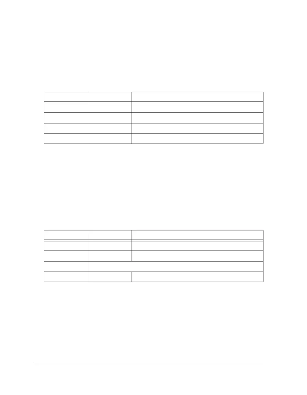
Table A-69. MLB_CCBCRx Register Bit Descriptions (RO)
Bit Name Description
1–0 Reserved for other channel types
15–2 BFA Buffer Final Address.
17–16 Reserved for other channel types
31–18 BCA Buffer Current Address.
Table A-70. MLB_CNBCRx Register Description (RW)
Bit Name Description
1–0 Reserved for other channel types
15–2 BEA Next Buffer End Address.
17–16 Reserved
31–18 BSA Next Buffer Start Address.

 Loading...

