ADSP-2146x External Port Registers
A-44 ADSP-214xx SHARC Processor Hardware Reference
DDR2 Pad Control Register 1 (DDR2PADCTL1)
The
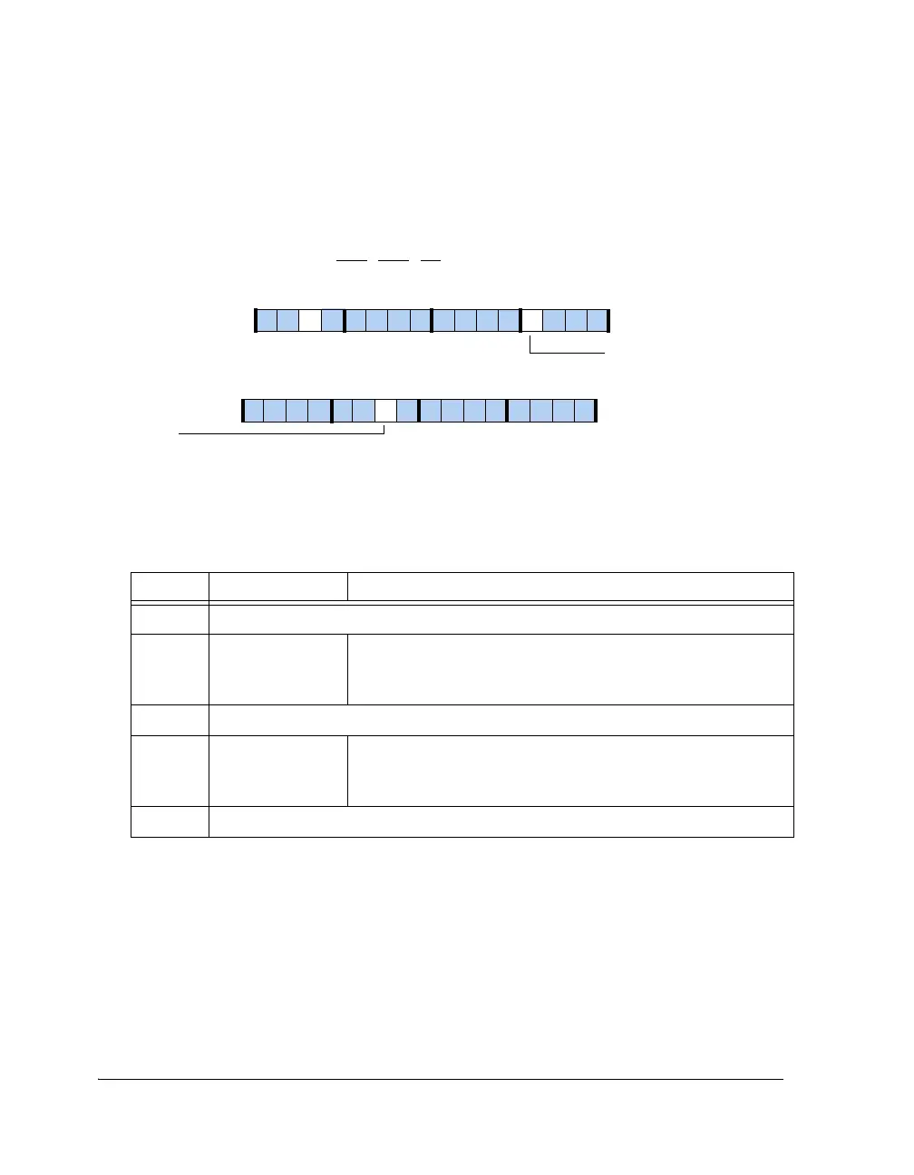
DDR2PADCTL1 register shown in Figure A-19 and described in
Table A-24 includes the programmable parameters associated with the
DDR2 Command (CS, CAS, RAS, WE, ODT) and Address pad control.
Figure A-19. DDR2PADCTL1 Register
Table A-24. DDR2PADCTL1 Register Bit Descriptions (RW)
Bit Name Description
8–0 Reserved
9 ADDR_PWD Address Pad Receiver Power Down.
0 = Normal mode
1 = Power-down mode
18–10 Reserved
19 CMD_PWD Command Pad Receiver Power Down.
0 = Normal mode
1 = Power-down mode
28–31 Reserved
31 302928 27 26 25 24 23 22 21 20 19 18 17 16
09 837564 2114 12 11 101315
ADDR_PWD
Receiver Power Down
CMD_PWD
Receiver Power Down

 Loading...

