Operating Modes
12-12 ADSP-214xx SHARC Processor Hardware Reference
Bypass Mode
When the BYPASS bit is set (=1), the input data bypasses the sample rate
converter and is sent directly to the serial output port. Dithering of the
output data when the word length is set to less than 24 bits is disabled.
This mode is ideal when the input and output sample rates are the same
and SRCx_FS_IP_I and SRCx_FS_OP_I are synchronous with respect to each
other. This mode can also be used for passing through non-audio data
since no processing is performed on the input data in this mode.
Matched-Phase Mode (ADSP-21488)
The matched phase mode of the sample rate converter is enabled by the
SRCx_MPHASE bit. This mode is used to match the phase (group delay)
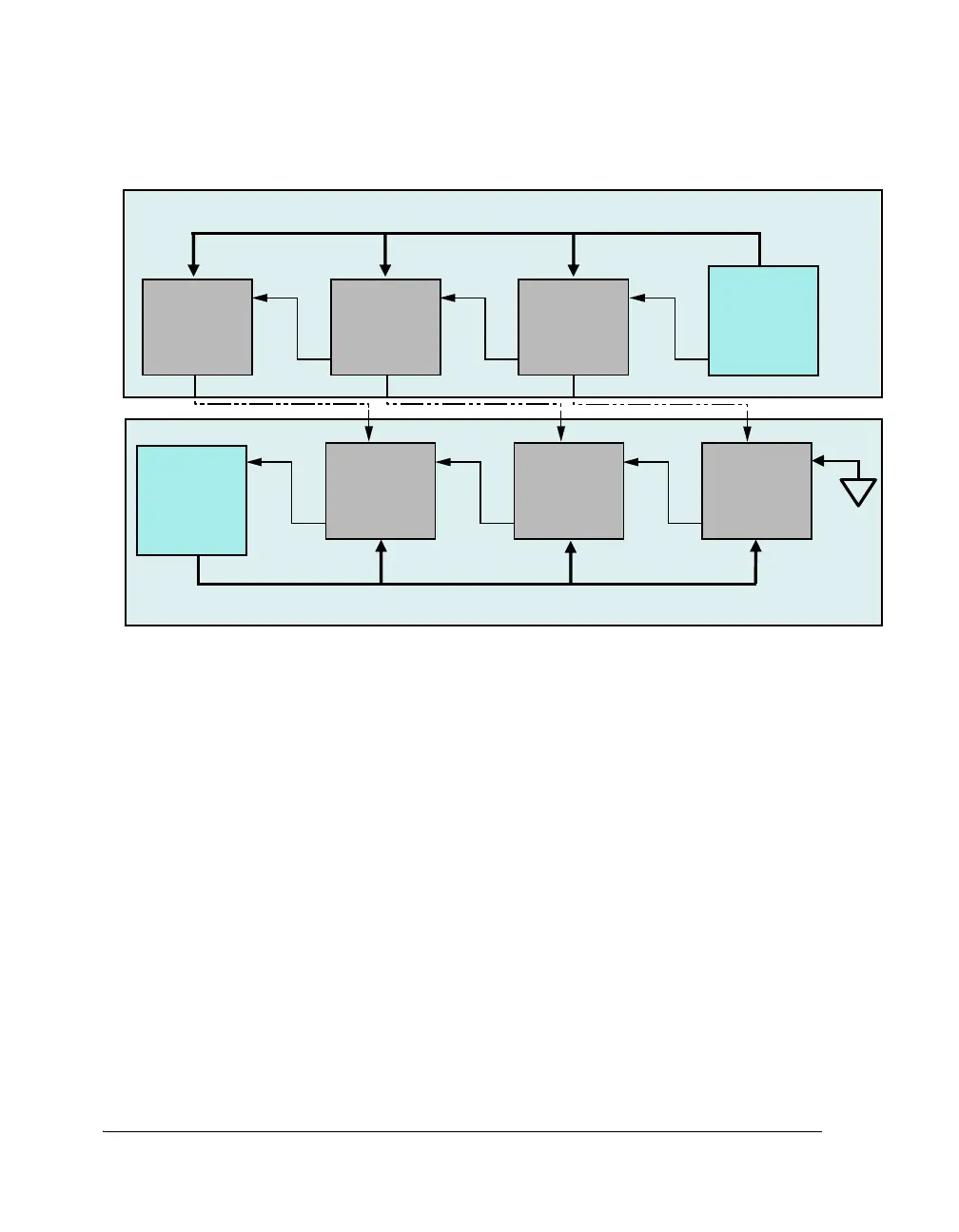
Figure 12-4. TDM Input/Output Modes
SRC2_DAT_IP_I
SRC2_TDM_IP_O
TDM IP Daisy Chain
TDM OP Daisy Chain
Clock, FS
Clock, FS
SPORT_Dx_O
MASTER
Tx
SRC1_DAT_IP_I
SRC1_TDM_IP_O
SRC0_DAT_IP_I
SRC0_TDM_IP_O
SRC2_TDM_OP_I
SRC2_DAT_OP_O
SRC1_TDM_OP_I
SRC1_DAT_OP_O
SRC0_TDM_OP_I
SRC0_DAT_OP_O
MASTER
Rx
SPORT_Dx_I

 Loading...

