ADSP-214xx SHARC Processor Hardware Reference A-25
Registers Reference
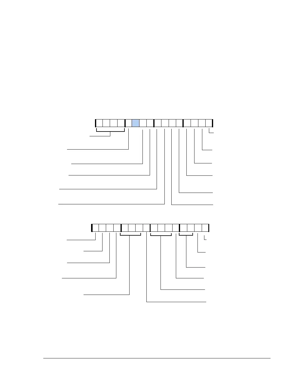
DDR2 Control Register 0 (DDR2CTL0)
The DDR
DDR2CTL0 register includes the programmable parameters asso-
ciated with the DDR configuration. Figure A-9 and Table A-11 show the
corresponding control bit definitions. The FEMRx, FLMR, FDLLCAL, FAR, FPC,
SREF_EXIT, DDR2SRF, and DDR2PSS bits are automatically cleared on the
next clock edge cycle after they are set.
Figure A-9. DDR2CTL0 Register
FLMR
Enable Pipeline
DDR2BUF
Force EMR Register Write
FEMR3
Force EMR3 Register Write
DDR2SRF
Force MR Register Write
DDR2ORF
Self Refresh Entry Mode
Disable Auto Refresh
Mode
FAR
Force Auto Refresh
FEMR
FPC
SREF_EXIT
Self Refresh Exit
Force Precharge
DIS_DDR2CTL
FDLLCAL
Force On-chip DLL
Calibration
FEMR2
Force EMR2 Register
Write
DIS_DDR2CLK1
Disable DDR2 Clock 1
DDR2 Enable
SH_DLL_DIS
Internal DLL Disable
DDR2RAW (11–9)
DDR2 Row Address Width
DDR2CAW (7–5)
Bank Column Address Width
DIS_DDR2CKE
DDR2 CKE Disable
DDR2BC (3–2)
DDR2 Bank Count
DDR2ADDRMODE
Address Mapping Mode
DDR2PSS
Powerup Start
DDR2OPT
Read Optimization Enable
DDR2MODIFY (3 1–28)
Read Modifier
31 302928 27 26 25 24 23 22 21 20 19 18 17 16
09 837564 2114 12 11 101315
DDR2WDTHx16
Must always be set to 1 for
ADSP-2146x.

 Loading...

