Peripherals Routed Through the DAI
A-196 ADSP-214xx SHARC Processor Hardware Reference
PCG Frame Synchronization Registers (PCG_SYNCx)
These registers, shown in Figure A-105, and Figure A-106 and described
in Table A-102 and Table A-103, allow programs to synchronize the clock
frame syncs units with external frame syncs.
Note the
CLKxSOURCE bits (PCG_CTLx1 register) are overridden if
CLKx_SOURCE_IOP bits (bit 2) in the PCG_SYNCx registers are set.
17 INVFSx Active Low Frame Sync Select.
0 = Active high frame sync
1 = Active low frame sync
31–18 Reserved (In bypass mode, bits 31–18 are ignored.)
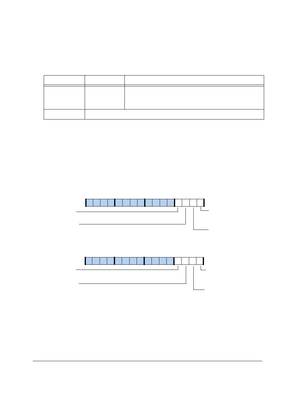
Figure A-105. PCG_SYNC1 Register
Table A-101. PCG_PWx Register Bit Descriptions
(in Bypass Mode) (RW) (Cont’d)
Bit Name Description
Enable Synchronization of
FSB with External LRCLK
FSB_SYNC
FSA_SOURCE_IOP
Enable FSA Input Source
Enable Synchronization of
FSA with External LRCLK
FSA_SYNC
Enable Synchronization of Clock
A with External LRCLK
CLKA_SYNC
CLKA_SOURCE_IOP
Enable Clock A Input Source
Enable Synchronization of
clock B with External LRCLK
CLKB_SYNC
FSB_SOURCE_IOP
CLKB_SOURCE_IOP
Enable Clock B Input Source
Enable FSB Input Source
31 302928 27 26 25 24 23 22 21 20 19 18 17 16
09 837564 2114 12 11 101315

 Loading...

